
LG Electronics is making a bold push into the high-end semiconductor equipment market, setting its sights on hybrid bonding (HB) tools, critical for producing next-generation high-bandwidth memory (HBM) chips. Often described by industry insiders as the "dream tool" for future memory packaging, HB systems are seen as essential to boosting performance in AI and data-intensive applications.
The initiative marks a pivotal shift for LG, aligning with the group's wider strategy to expand its footprint in artificial intelligence and business-to-business (B2B) markets.
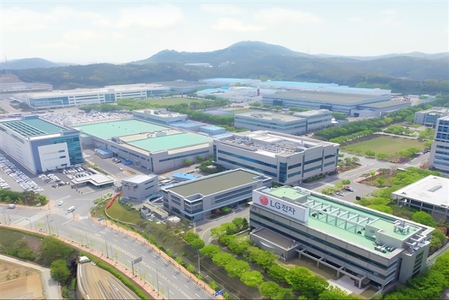
According to Seoul Economic Daily, LG's Production Research Institute (LG PRI) has begun developing HB tools, aiming for mass production readiness by 2028. The company has confirmed that R&D is underway, highlighting its intention to challenge established players in this emerging but strategically vital segment of the semiconductor supply chain.
Strategic move aligned with AI and B2B expansion
Industry analysts interpret LG's recent strategic shift as aligning with Chairman Koo Kwang-mo's overarching plan to steer the conglomerate toward emerging technologies. The company has intensified its focus on artificial intelligence and business-to-business ventures, aiming to establish foundational infrastructure that supports long-term digital transformation beyond the scope of consumer goods.
This move places LG in direct technological rivalry with prominent South Korean firms like Samsung Electronics, Hanwha Semitech, and Hanmi Semiconductor, which are already engaged in developing or supplying equipment for HBM production.
Building out semiconductor packaging capabilities
Reports indicate that LG PRI has recently formed a new division focused on advanced semiconductor packaging technologies. With the development of HB tools now underway, industry watchers expect LG to significantly scale this unit, recruit top talent in semiconductor packaging, and deepen collaborations with academic institutions.
Earlier coverage by ET News noted that LG PRI is also developing other advanced tools, including Laser Direct Imaging (LDI) systems for IC substrates and Through-Glass Via (TGV) laser drilling equipment for glass-based substrates, laying the groundwork for a comprehensive advanced packaging equipment portfolio.
Hybrid bonding could reshape HBM landscape
Hybrid bonding is emerging as a game-changing alternative to traditional thermo-compression bonding (TCB), offering a more advanced method for vertically stacking semiconductor chips. Unlike TCB, which relies on micro bumps to link chips, hybrid bonding allows for direct die-to-die connections without the need for bumps. This innovation enables thinner chip assemblies and improved thermal performance, both critical for the densely stacked DRAM layers found in HBM.
Although hybrid bonding is already used in NAND flash and some system-on-chip applications, it has yet to be widely adopted for HBM production. LG's entry into this space could accelerate that shift, especially as the company seeks to boost profitability through a deeper push into business-to-business technologies.
If successful, LG could secure contracts with leading HBM manufacturers such as SK Hynix, Micron, and Samsung. Such wins would strengthen LG's position in the semiconductor equipment industry and drive growth in a sector vital to next-generation AI and computing applications.
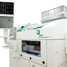
Credit: Besi
Korean players challenge global HB leaders
The current hybrid bonding equipment market is dominated by the Netherlands-based BE Semiconductor Industries (Besi) and the US-based Applied Materials. But with SK Hynix and Samsung leading the global HBM supply, South Korean firms are eager to localize this strategically important technology. Industry watchers say LG could gain traction if it meets the stringent performance and reliability demands of top-tier chipmakers.
Samsung is reportedly preparing to deploy hybrid bonding for its sixth-generation HBM, known as HBM4, as early as 2025. SK Hynix may adopt the technology for its next-generation HBM4E products. Samsung's affiliate Semes is also developing in-house hybrid bonding systems to support the company's HBM roadmap.
Meanwhile, Hanwha Semitech, which currently supplies TCB systems to SK Hynix, is rapidly expanding its hybrid bonding capabilities. The company views fast commercialization as a critical path to future competitiveness.
Hanmi Semiconductor, another major TCB supplier to SK Hynix, recently unveiled plans to invest KRW28.5 billion (US$20.8 million) in a new hybrid bonding equipment factory. The move further intensifies the race among Korean firms to gain the upper hand in one of the semiconductor industry's most promising new frontiers.
Article translated by Sherri Wang and edited by Jerry Chen

