

SK Hynix is targeting 2028 to apply High-NA extreme ultraviolet lithography to DRAM mass production and is considering joining an industry initiative to develop 12-inch photomasks, according to South Korea's fnnews. The company has separately confirmed both plans.
The target puts SK Hynix on a similar timetable to Samsung Electronics, which plans to introduce ASML's High-NA EUV technology into future DRAM high-volume manufacturing by 2028.
The parallel roadmaps set up the next stage of competition between South Korea's two leading memory makers as they push DRAM scaling beyond conventional EUV. The key challenge will be turning High-NA's higher resolution into a stable and economically competitive manufacturing process.
High-NA becomes next DRAM scaling step
High-NA raises the numerical aperture of EUV lithography systems from 0.33 to 0.55, enabling finer patterning as semiconductor geometries shrink.
For DRAM manufacturers, the technology offers a potential path to simplify increasingly complex EUV process flows while extending device scaling. Samsung expects the higher resolution to support process simplification and greater manufacturing efficiency, while SK Hynix plans to use the technology to accelerate next-generation memory development and improve product and cost competitiveness.
The economics, however, will depend on more than resolution. Throughput, process maturity, yield, and equipment costs will determine how quickly High-NA can deliver an advantage in volume manufacturing.
SK Hynix has already begun building the infrastructure needed for High-NA development.
The company first introduced EUV into its fourth-generation 10nm-class, or 1a, DRAM process in 2021 and has since expanded the technology across advanced DRAM manufacturing.
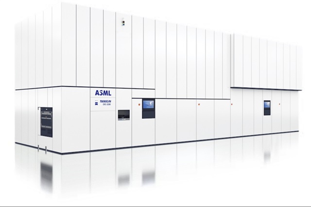
In September 2025, SK Hynix assembled ASML's TWINSCAN EXE:5200B High-NA EUV system at its M16 fab in Icheon. The EXE:5200B is the first model designed for volume production in ASML's High-NA product line.
The increase in numerical aperture to 0.55 enables the system to print features 1.7 times smaller and support transistor densities 2.9 times higher than conventional EUV equipment.
The 2028 target now gives SK Hynix a timetable for moving from equipment installation and process development toward DRAM volume production.
Samsung is moving along a similar path. Its expanded collaboration with ASML covers High-NA EUV and other advanced manufacturing technologies, including infrastructure for the future transition to larger photomasks.
Neither company has specified which DRAM generation will first adopt High-NA, making it premature to tie the 2028 plans to a particular DRAM node. The timelines also remain targets rather than confirmed production start dates.
12-inch masks follow on a longer timeline
Alongside the High-NA race, the industry is preparing for a separate transition from today's 6-inch photomasks to a 12-inch format.
ASML and TSMC established an industry-wide initiative on September 7 to develop the larger masks. Samsung has joined the initiative, while SK Hynix is evaluating participation.
The initiative aims to establish a 12-inch mask pilot line by 2031 and support full lithography-system readiness for advanced-node production by 2033.
That timetable is separate from Samsung's and SK Hynix's 2028 DRAM plans. Their initial High-NA EUV production is expected to use existing 6-inch masks, allowing the companies to adopt the lithography technology before the larger-mask ecosystem is ready.
TSMC plans to introduce High-NA into high-volume manufacturing for advanced nodes beginning in 2030.
The push toward larger masks addresses one of the trade-offs associated with High-NA lithography. Its anamorphic optical architecture delivers higher resolution but reduces the maximum single-exposure field compared with conventional EUV, creating stitching constraints when manufacturing very large dies.
The limitation matters most for processors approaching the maximum exposure area, including large data center chips. Current EUV systems can accommodate dies of roughly 800 square millimeters, close to the size of some of the industry's largest processors.
Moving to 12-inch masks is intended to reduce stitching constraints, increase scanner productivity, and lower manufacturing costs. ASML estimates that system productivity could eventually improve by about 40% if the industry successfully completes the transition.
For DRAM, stitching is generally less immediate a concern than it is for the largest logic processors. The nearer-term significance for Samsung and SK Hynix is therefore High-NA's ability to extend memory scaling rather than the larger-mask format itself.
Samsung's participation, and SK Hynix's potential participation, would also position the two memory makers to take part in developing the lithography infrastructure and standards expected to support wider High-NA adoption in the 2030s.
2028 puts execution in focus
The industry's High-NA roadmap is now separating into two clear phases.
Samsung and SK Hynix are targeting High-NA DRAM manufacturing around 2028 using existing mask infrastructure. TSMC plans to bring the technology into advanced-node high-volume manufacturing in 2030, followed by the 12-inch mask pilot line in 2031 and readiness for High-NA production systems using 12-inch masks in 2033.
For the Korean memory makers, the first contest will therefore come before the mask transition.
With both targeting 2028, the next DRAM scaling race will increasingly be determined by how quickly each company can turn High-NA from advanced lithography equipment into a mature volume-production process.
Article edited by Ysi Chen
