

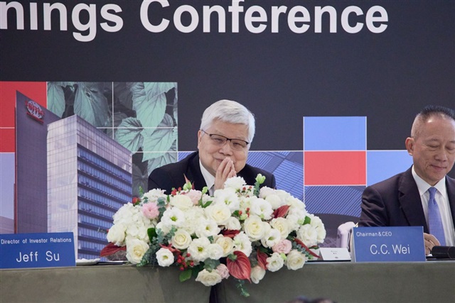
TSMC chairman C.C. Wei recently visited Japan and appeared alongside Prime Minister Sanae Takaichi to jointly announce that Kumamoto Fab 2 will be upgraded from a 6nm to a 3nm process, signaling Japan's plan to reclaim its semiconductor glory. However, according to supply chain sources, when the Japanese government first invited TSMC to build fabs in Kumamoto, it had already mapped out three major strategies that included advancing advanced packaging and constructing new facilities. Most importantly, Japan aims to leverage its strengths in equipment and materials to reinforce its critical position and bargaining power in the advanced packaging industry chain.
Early talks stalled
It is clear that Japan understands its domestic limitations and needs TSMC's support. When plans for Kumamoto Fab 2 first surfaced in 2023, there were simultaneous reports that the Japanese government hoped TSMC would also add advanced packaging capacity. At the time, Kumamoto had no solid plan below 7nm, AI demand was just taking off, and TSMC did not yet have a full grasp of advanced packaging supply and demand, so the idea faded. Given that Kumamoto Fab 2 upgraded to 3nm, the proposal to invite TSMC to establish an advanced packaging plant in Japan has resurfaced. TSMC's spokesperson declined to comment on market rumors.
Regaining influence
Although Japan does not dominate wafer foundry or IC design, it wields significant influence in the global semiconductor supply chain, particularly in equipment and materials. In the silicon wafer market, Shin-Etsu Chemical and SUMCO together hold more than half of global market share. In addition, major Japanese companies such as Ibiden, TOK, JSR, Fujifilm, Sumitomo Chemical, Nitto, SCREEN, Tokyo Electron (TEL), and Advantest are key partners of TSMC, Intel, and Samsung Electronics. It is committed to reclaiming its semiconductor prominence. In response to rising geopolitical risks, Japan began rebuilding its upstream, midstream, and downstream manufacturing capabilities years ago. Japan invested heavily in bringing in TSMC's support for wafer manufacturing, while making a massive investment in Rapidus.
Deepening ties to strengthen ecosystem
By leveraging its strengths, Japan recently succeeded in having TSMC revise Kumamoto Fab 2's manufacturing roadmap, upgrading it from 6nm directly to 3nm. TSMC established a Japanese subsidiary in 1997, set up a technology center in Yokohama in January 2020, and founded a 3D IC R&D center in March 2021. Working with more than 20 Japanese partners, including Ibiden and Shin-Etsu Chemical, the total investment reached JPY37 billion (US$236.1 million), with TSMC contributing JPY18 billion and the Japanese government JPY19 billion. The Kumamoto fab is also a joint venture with Sony and other Japanese firms, with strong government subsidies.
The missing link
Without corresponding advanced packaging mass production capacity, even if advanced processes reach the 3nm generation, chips would still need to be packaged overseas, significantly weakening supply chain autonomy. Several years ago, the Japanese government repeatedly proposed the idea of establishing advanced packaging facilities locally with TSMC, hoping to form a complete manufacturing plus packaging cluster that would drive upgrades across substrates, chemical materials, and equipment suppliers. Given the explosive demand for AI chips and surging needs for technologies such as CoWoS, related proposals have been revived. Building advanced packaging facilities is not difficult for TSMC, but sufficient order volume is critical. Because of Japan's strengths in equipment and materials, along with its willingness to offer generous subsidies to develop AI applications, TSMC has been evaluating the opportunity.
ASE and domestic alliances
In addition to TSMC, ASE Group announced in 2024 an investment of about NT$700 million (US$22.1 million) to establish a production base in Kitakyushu, Japan, and has been aggressively expanding advanced packaging capacity and advancing technology in recent years. It is also rumored to be one of the Japanese government's cooperation partners. However, ASE's spokesperson stated that the company has not yet received any further invitations from the Japanese government.
Japan has also made early preparations in advanced packaging by actively establishing advanced packaging development hubs that integrate materials and equipment suppliers as well as academia into technical application alliances. Domestic companies have jointly formulated strategies to develop next-generation equipment and materials, while working with local IDMs and foundries to propose technology upgrade paths. Japan has been investing heavily in R&D for 2.5D/3D packaging and hybrid bonding. Because domestic OSAT players and alliances are relatively small in scale, Japan has also been actively participating in international alliances in recent years to strengthen its capabilities.
Outside of Taiwan, TSMC is potentially planning for even more advanced packaging plants in the US, adding more pressure on Japan's semiconductor policymakers. With strong Taiwan–Japan relations and Japan's control over key equipment and materials, TSMC's deployment in Japan is likely to become broader and deeper.
Article translated by Emily Kuo and edited by Joseph Tsai