

The Institute of Physics of Microstructures of the Russian Academy of Sciences (IPM RAS) has recently announced a long-term roadmap for the development of an extreme ultraviolet (EUV) lithography system. The plan aims to create a Russian-made EUV machine operating at an 11.2nm wavelength.
Dmitry Kuznetsov, a computer data science PhD, shared the project roadmap on X. It is a continuation and concrete elaboration of ideas first revealed in December 2024 and is seen as a crucial step in Russia's efforts toward self-sufficiency in chip manufacturing. The timeline spans from 2026 to 2037, covering technologies from 40nm down to below 10nm.
A different technical path
Unlike the EUV systems from Dutch semiconductor equipment supplier ASML, Russia's approach employs an entirely different architecture, including a hybrid solid-state laser, a xenon plasma light source, and mirrors made from ruthenium/beryllium (Ru/Be) to reflect light at the 11.2nm wavelength.
The choice to avoid ASML's tin droplet plasma light source stems from the reduced optical contamination and maintenance requirements associated with xenon plasma. This architecture avoids high-pressure immersion fluids and multi-patterning steps, resulting in a simplified system with lower maintenance costs.
Three-phase development timeline
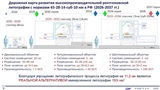
According to the roadmap, Russia's indigenous EUV development will proceed in three stages:
Stage 1 (2026–2028): Focus on developing a prototype system supporting 40nm process nodes, using a dual-mirror optical system, with 10nm overlay accuracy. The exposure area will be 3x3mm, capable of processing more than 5 wafers per hour.
Stage 2 (2029–2032): Development of a 28nm scanner with a four-mirror design, expandable to 14nm. Overlay accuracy will improve to 5nm, with a maximum exposure area of 26x0.5mm, and throughput exceeding 50 wafers per hour.
Stage 3 (2033–2036): Aiming to support sub-10nm nodes, utilizing a six-mirror configuration. Overlay accuracy will improve to 2nm, exposure area up to 26x2mm, with throughput surpassing 100 wafers per hour.
Lower costs, but major hurdles remain
Reports state that the Russian EUV system is expected to support process nodes from 65nm down to 9nm, meeting most key manufacturing needs from 2025 through 2030. Manufacturing costs are projected to be significantly lower than those of ASML's Twinscan NXE and EXE platforms, making the system suitable for small and medium-sized fabs rather than exclusively for large-scale manufacturers.
However, the industry is skeptical about the feasibility of the technology. The use of a non-standard 11.2nm wavelength requires redesigning core components such as optical systems, laser light sources, mirror polishing equipment, and photoresist materials—each posing major technical challenges.
There is currently no evidence that Russia possesses the manufacturing capability to mass-produce key EUV components, such as reflective mirrors or high-power light sources.
Analysts have also noted that the roadmap represents Russia's attempt to bypass Western technological restrictions and achieve semiconductor self-sufficiency through EUV development, but whether this ambition can be fully realized remains questionable. Even if partially successful, the project could offer an alternative mid-to-high-end lithography solution for countries outside the ASML ecosystem, potentially reducing global dependence on a single equipment supplier.
Credit: X
Article translated by Emily Kuo and edited by Jerry Chen

