In 2020, Samsung Electronics had a monthly capacity of 260,000 wafers for its 8-inch and 12-inch fabrication each, which increased to 265,000 and 325,000 respectively in 2021. It is estimated that its 12-inch fab capacity will increase to 443,000 wafers in 2022, with 5/7nm capacity increasing to 60,000 (compared to 30,000 as of the end of 2020). Samsung has committed to steady investment in the foundry business until 2026, but the biggest challenge for Samsung's foundry business is the fact that the captive market's contribution is very high.
In 2020, Samsung's foundry relied on internal orders for 60% of its sales and more than 50% in 2021. Qualcomm (25%) and Nvidia (13%) were the two largest external customers, with their combined share reaching nearly 40%, and other companies contributing about 10% together. According to Korean media reports, Samsung's own application processors (AP) contributed 21% of sales, CIS about 15%, DDI about 10%, but in terms of profit, the AP proportion was the highest, followed by the use of 65nm technology-made GPUs, CIS and DDI, which together accounted for only about 10% of the profit contribution.
According to UBS estimates, System LSI division's contribution to Samsung's profits will increase from 3% in 2021 to 6% in 2022 and remain at 6-8% until 2026.
Samsung's 12-inch foundry capacity is expected to grow 3.2 times between 2017 and 2026, with its US$17 billion project to build a semiconductor manufacturing facility in Taylor, Texas breaking ground in 2022 and launching operation in the second half of 2024. UBS estimates that Samsung's foundry business will spend US$13 billion in capital expenditure in 2022, a significant rise from US$3.4 billion in 2018. It is estimated that annual capex will be around US$16 billion for the next few years.
Samsung's foundry business is now highly dependent on the mobile communications sector, which occupies a share of over 60%, while high efficiency computing (HPC) accounts for only 10% or less. It is a challenge for Samsung to raise the sales contribution of HPC.
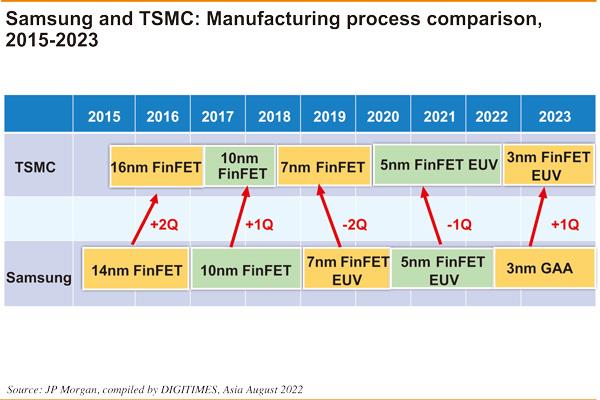
Samsung's 5nm yield rate is likely to have reached over 70%; there is still much room for improvement for 4nm manufacturing; but the new 3nm GAA process, without the baggage of the past, should fare much better. The 3nm GAA process, dubbed 3GAE, will only be used for crypto chip production in 2022. The second-generation 3GAP process is more meaningful, but the commercialization may not take place until 2024, and the HPC customers using 3GAP may only enter mass production in 2024-2025.
Samsung believes that HPC customers need a second supplier, so in addition to TSMC, they will choose between Samsung and Intel. Samsung even hopes to join forces with Intel to break TSMC's dominance in advanced node manufacturing. For investment in the US, the tax incentives and proximity to local clients may be attractive, but if Samsung cannot surpass TSMC in advanced processes, it will be difficult to obtain sufficient returns on its investments in the US.
(Editor's note: This is part of a series of 10 articles by DIGITIMES Asia president Colley Hwang about Samsung's outlook.)