
Global semiconductor companies are discussing relaxing thickness standards for next-generation high-bandwidth memory (HBM) as the industry moves toward higher stack counts in future designs, according to ZDNet Korea.
HBM has become a key component of artificial intelligence (AI) computing infrastructure, and competition between Samsung Electronics and SK Hynix in the HBM4 market is intensifying as both companies develop next-generation memory technologies.
JEDEC revisits thickness limits for next-gen HBM
Companies participating in the semiconductor standards body JEDEC are discussing significantly relaxing thickness standards for future HBM products that may require stacking up to 20 layers of DRAM.
HBM4, the sixth generation of HBM scheduled for commercial deployment this year, has a thickness of 775 micrometers. Industry discussions are considering raising the standard to roughly 825 to 900 micrometers or more.
HBM vertically stacks multiple DRAM dies and connects them through fine microbumps. Thickness standards remained at 720 micrometers through the HBM3E generation but increased to 775 micrometers for HBM4 as DRAM stacking expanded from 8 and 12 layers to 12 and 16 layers.
Looking ahead, the industry is discussing relaxing thickness limits for next-generation products such as HBM4E and HBM5, which may stack as many as 20 DRAM layers. Current proposals range from 825 micrometers to more than 900 micrometers.
A source familiar with the matter said JEDEC typically establishes key standards about one to one and a half years before commercial production, adding that discussions on next-generation HBM thickness are already underway.
JEDEC defines semiconductor and memory standards and includes memory manufacturers such as Samsung Electronics, SK Hynix, and Micron, as well as major chip companies including Intel, TSMC, Nvidia, and AMD.
Packaging shifts fuel the debate
The semiconductor industry has traditionally imposed strict limits on HBM thickness. If memory packages become too thick, aligning them with system semiconductors such as GPUs integrated alongside them becomes more difficult. Increased spacing between DRAM layers can also lengthen data transmission paths, potentially affecting performance and efficiency.
To address these constraints, memory manufacturers have adopted several approaches to control package thickness, including die-thinning processes that grind down the back side of DRAM chips and bonding technologies designed to reduce spacing between stacked DRAM dies.
Despite these efforts, the move toward 20-layer HBM stacks is exposing technical limits in existing thinning and bonding methods.
Packaging developments at foundries are also contributing to the discussion. TSMC currently dominates the 2.5D packaging process known as CoWoS, which integrates HBM and GPUs into a single AI accelerator using a large interposer placed between the chips and the substrate.
The next step in TSMC's packaging roadmap is SoIC (System-on-Integrated Chips), a technology that vertically stacks system semiconductors with very fine spacing. In AI accelerators using TSMC-SoIC, stacked system chips are combined with HBM.
When SoIC is applied, system semiconductor packages are expected to become tens of micrometers thicker than the current 775 micrometers, creating pressure for HBM thickness standards to be relaxed. Nvidia and Amazon Web Services are reportedly planning to adopt TSMC-SoIC.
Another source said demand for relaxing HBM thickness standards is emerging not only from memory suppliers but also from foundries, though it remains uncertain whether such proposals will ultimately be adopted.
Hybrid bonding hits a wall
Industry observers say relaxing thickness standards could reduce the urgency to adopt newer bonding approaches such as hybrid bonding.
Bonding refers to the process of connecting individual DRAM dies inside an HBM stack. The dominant method today is thermo-compression (TC) bonding, which uses heat and pressure to attach chips.
Hybrid bonding directly connects copper wiring between chips or wafers, eliminating microbumps and allowing DRAM spacing to approach zero. This can significantly reduce overall package thickness.
However, hybrid bonding presents technical challenges. It requires removing microscopic contamination from chip surfaces, achieving extremely smooth surfaces through chemical mechanical polishing (CMP), and maintaining high alignment precision between copper pads. Yields can also decline sharply when bonding up to 20 chips within a single stack.
As a result, memory manufacturers continue to research hybrid bonding but have not yet applied it to mass production of HBM. Even Samsung Electronics, which is actively developing the technology, is expected to introduce hybrid bonding only partially and at the earliest in 16-layer HBM4E products.
If thickness standards are relaxed, memory companies may continue mass-producing HBM using existing TC bonding equipment.
A source said some in the sector believe relaxing thickness limits by more than 50 micrometers would already make it possible to implement 20-layer HBM. Even if hybrid bonding is introduced in the future, replacing existing equipment would require substantial investment, making memory manufacturers generally supportive of easing thickness restrictions.
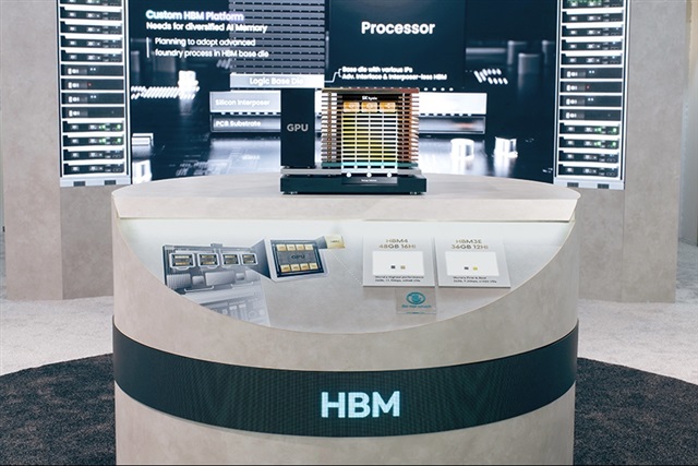
SK Hynix puts 16-layer HBM4 on display
SK Hynix recently showcased a 16-layer HBM4 product with a capacity of 48GB at its customer exhibition hall at the Venetian Expo in Las Vegas, ETNews reported.
The product follows a 12-layer 36GB HBM4 device capable of speeds of 11.7Gbps. By stacking 16 layers of DRAM, the new product increases both capacity and performance, delivering bandwidth exceeding 2TB per second.
A company representative said the firm has begun providing samples to customers and plans to supply the product according to customer demand.
The company also outlined its long-term "custom HBM" strategy, which incorporates Stream DQ technology designed to process data directly within DRAM to reduce computational overhead on GPUs.
Other memory technologies displayed included SOCAMM2 low-power memory modules for AI servers and LPDDR6 products optimized for on-device AI.
In NAND flash, the company presented a 321-layer 2Tb QLC product designed for high-capacity enterprise SSDs used in AI data centers. Compared with previous QLC generations, the device improves density, power efficiency, and performance.
Article edited by Jerry Chen