

As AI workloads move from cloud to edge, the volume of image and sensor data across industries is rising rapidly. Edge devices that previously relied on FPGAs and off-the-shelf modules are now running into combined constraints in power, latency, and cost. As models evolve from simple classification to more complex scene understanding, compute density at the edge has increased significantly over the past two years. Many startups and SMEs in the United States and China report that existing platforms can no longer support large-scale deployment.
To address this pain point, Progate Group Corporation (PGC) has launched its Design Service Turnkey Platform to help customers migrate from FPGA-based acceleration to ASIC-based architectures.
While most edge AI systems ultimately ship as system-on-chip (SoC) solutions, the ability to implement a dedicated ASIC architecture on the right process node - combining high compute density, low power consumption, and long-term supply – has become a critical condition for scaling edge AI.
As a member of the TSMC Design Center Alliance (DCA), PGC has more than 30 years of experience on TSMC processes, with a strong track record in ASIC design, tape-out, and mass production on 22 nm, 12 nm, and 6 nm. The company has also built front-end and back-end design capabilities that extend to 3 nm. On these complex nodes, PGC provides its PGC Design Service Turnkey Platform to help customers bring edge AI SoCs into the ASIC phase in a more controlled and predictable way.
Vision Inference AI SoCs: The Earliest Edge Workloads to Move to ASIC
Image inference workloads, driven by high-bandwidth and continuous data streams, are rapidly pushing the limits of FPGAs and general-purpose modules. As model complexity increases, latency, throughput and memory bandwidth have become the primary performance bottlenecks.
Industry research indicates that there are already more than 200 startups in the United States focused on edge computing and computer vision, while over 100 companies in China are working on smart city, community surveillance, and industrial vision applications. Global forecasts further suggest that by 2030, vision-centric workloads will account for nearly half of the edge AI market and will be among the first segments to complete the transition from FPGAs and commercial modules to ASIC-based solutions.
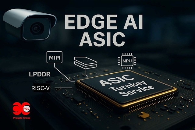
As edge AI expands across home, retail, logistics, urban infrastructure, and industrial control, requirements for low power, millisecond-level latency, stable memory bandwidth, and long-term component availability are becoming stricter. The success of an edge AI SoC therefore depends not only on advanced process nodes, but also on whether it integrates the right memory subsystem, high-speed I/O interfaces, and security modules and IP, so that the SoC can be fully optimized as an ASIC.
Within the TSMC DCA ecosystem, advanced nodes are already showing a clear division of roles. 22ULP is well suited for battery-powered and long-standby home and outdoor devices. For edge AI devices on 22 nm, TSMC also offers embedded RRAM (ReRAM) to balance cost and yield. 7 nm and 6 nm nodes provide the integration density required to combine ISP, vision DSP, RISC-V cores, AI accelerators (NPU), memory subsystems (including memory controllers and DRAM PHYs), and security modules, making them preferred nodes for high-end edge ASICs.
As resolutions and model complexity increase, LPDDR4X and DDR4 remain the mainstream memory for a large portion of edge cameras, while higher-end applications are moving to LPDDR5 to secure additional bandwidth. Whether these IP blocks can be integrated into a low-latency, high-throughput data path will directly determine whether a product can move from proof of concept (PoC) to stable volume production.
PGC: An Integrated ASIC Design Service Turnkey Platform for Process, IP, and Supply Chain
PGC’s Design Service Turnkey Platform is built as an integrated design service environment. Through the Synopsys IP OEM Program, PGC provides more competitive IP cost and licensing models, and can deliver complete memory subsystems for LPDDR5/LPDDR4X/DDR (including memory controllers and DRAM PHYs), as well as MIPI CSI-2/D-PHY image interface IP and PCIe high-speed I/O. The platform also supports low-latency architectures and security modules required by edge AI SoCs.
At the same time, PGC maintains long-term collaboration with ASE and other OSAT partners. This allows the company to support the full flow from front-end design, back-end APR, design signoff, and tape-out, through small-volume, multi-project wafer (MPW/CyberShuttle) runs, all the way to NTO and high-volume production, ensuring stable capacity across different product phases.
As edge AI gradually moves from product concepts to large-scale deployment, PGC will continue to deepen its integration of TSMC wafer processes, Synopsys IP, and ASE OSAT capabilities. The goal is to help startups and small to mid-sized companies around the world implement their edge AI ASIC strategies in a more efficient and controllable way, maintain long-term competitiveness through future technology transitions, and ultimately enable customer success.
