


Kevin Zhang, Deputy Co-Chief Operating Officer at TSMC, recently reiterated the company's cautious approach toward adopting High NA EUV lithography tools, emphasizing that TSMC is "in no rush" to bring the advanced technology into high-volume production. His remarks have reignited industry speculation around ASML's multi-billion-dollar next-generation lithography platform.
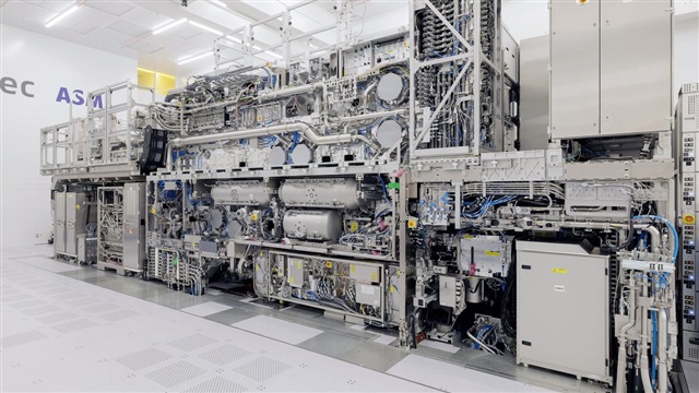
According to ASML, assembling a single High NA EUV system is a global logistical feat. The system's four main modules are manufactured in multiple locations across the US, Germany, and the Netherlands. These components are then shipped to ASML's Veldhoven headquarters, where they are assembled, tested, and certified—only to be disassembled once again for delivery to fabs in Asia or the US The shipping process alone requires either seven partially loaded Boeing 747 freighters or at least 25 large trucks.
Credit: ASML
At present, the majority of EUV shipments consist of the standard models, while deliveries of the High NA EUV machines remain limited.
Source: ASML; compiled by DIGITIMES, June 2025
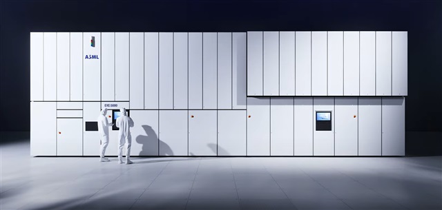
ASML unveils its colossus: 'larger than a double-decker bus'
Behind the tightly secured doors of a sprawling Dutch facility, ASML is showcasing a machine it believes will rewrite the future of semiconductor manufacturing. Nearly a decade in the making and priced at over US$400 million, the High NA EUV system is the most advanced—and most expensive—chipmaking tool ever built.
In a rare moment of transparency, ASML recently granted CNBC exclusive access to its lab, marking the first time the High NA EUV system has been filmed. Even ASML's internal teams have seldom had such up-close access to the fully assembled machine.
Assia Haddou, head of the High NA EUV certification team, described the system as "larger than a double-decker bus," built from four modular components constructed in Connecticut, California, Germany, and the Netherlands. Final assembly, testing, and certification take place in Veldhoven. The system's scale and complexity make logistics a feat unto itself.
Credit: ASML
TSMC: High NA can wait—Standard EUV still has room to run
While Intel has already deployed High NA EUV systems in its R&D pipeline for the Intel 18A process node, TSMC is opting for a more deliberate approach. Zhang confirmed that even the company's most advanced nodes—A14 (1.4nm-class) and A16 (1.6nm-class)—will not utilize High NA EUV in the near term.
"Everyone's curious when TSMC will deploy High NA EUV," Zhang said at TSMC's European Technology Symposium in late May. "The answer is simple: we'll adopt it when it delivers meaningful, measurable benefits."
Until then, TSMC's engineers are working to stretch the capabilities of current standard NA EUV systems, extending their lifespan and extracting more value. The SemiWiki community has described this confident approach as an example of TSMC's technological "arrogance"—in the best possible sense.
ASML's confidence undeterred: "All EUV customers will eventually adopt High NA"
Despite TSMC's measured stance, ASML remains optimistic about widespread adoption. CEO Christophe Fouquet has already secured commitments from the world's three leading logic chipmakers—Intel, TSMC, and Samsung—for High NA EUV systems. Intel, notably, has doubled down, recently installing a second High NA system at its R&D fab in Oregon. The company reports that the tool is meeting expectations and progressing steadily toward production readiness.
Fouquet continues to emphasize Intel's importance, calling it a cornerstone customer and a key player in maintaining US semiconductor independence, despite the firm's recent struggles.
Still, the barrier to entry remains steep. To date, only five High NA EUV machines have been delivered globally. But ASML is undeterred, projecting that every current EUV customer—including memory giants Micron and SK Hynix, as well as Japan's Rapidus—will eventually transition to High NA EUV.
ASML plans to ship at least five additional High NA tools in 2025 and aims to scale annual production to 20 units in the coming years.
The Immersion DUV refers to the ArFi lithography machines. Source: ASML; compiled by DIGITIMES, June 2025
Arizona fab may accelerate TSMC's timeline
While TSMC has yet to integrate High NA into its mainstream roadmap, ASML is betting that demand will soon materialize—especially from TSMC's new Arizona fab, which has officially entered volume production and now stands as the most advanced semiconductor plant on US soil.
In anticipation, ASML is constructing its first US-based training center in Arizona. Scheduled to open in the second half of 2025, the facility will train up to 1,200 EUV and DUV engineers annually. According to Fouquet, the center is designed not only to support US chipmaking ambitions but also to cultivate global talent.
Onward to Hyper NA: ASML's next moonshot
Looking further ahead, ASML is already sketching blueprints for the next frontier: Hyper NA EUV. Fouquet disclosed that preliminary optical designs are complete and the system's manufacturing complexity may not be as formidable as feared. He predicts demand for Hyper NA will emerge sometime between 2032 and 2035.
Article translated by Sherri Wang and edited by Jack Wu