

As artificial intelligence (AI) continues to reshape industries worldwide, the demand for smarter, faster, and more efficient electronic systems has never been greater. AI-enabled applications-from data center accelerators to compact edge devices-require processing systems with exceptional computational power, high performance, and access to large memory storage.
To meet these demands, the semiconductor industry is making rapid strides in advanced packaging technologies. These innovations are now central to system integration and architectural breakthroughs-yet they also introduce new challenges in reliability, thermal management, and multi-chip assembly.
Material companies are transforming their offerings to meet the stringent purity, precision, and performance requirements of the evolving semiconductor industry, while also creating more sustainable and environmentally friendly products. In this exclusive interview with Mr. Kenji Kuriyama, Director of Electronics for Japan & Taiwan at Henkel Adhesive Technologies, we explore how Henkel is helping semiconductor leaders overcome these challenges through materials innovation, strategic collaboration, and a deep commitment to Taiwan's ecosystem.
Mr. Kuriyama shares his optimistic outlook on the explosive growth of the advanced packaging market. In particular, Taiwan's semiconductor industry stands out as a global leader in advanced node manufacturing, producing the majority of the world's most sophisticated chips. Henkel looks forward to working closely with customers in Taiwan to accelerate the development of high-performance chips that drive AI innovation.
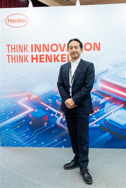
Mr. Kenji Kuriyama Director, Japan & Taiwan, Henkel Adhesive Technologies Electronics.
Credit: Henkel
Henkel Adhesive Technologies' Electronics division maintains a strong and deliberate focus on both the semiconductor and consumer electronics sectors, supplying advanced materials for electronics assembly, semiconductor packaging, and thermal management. Its product portfolio includes solutions for die attach, underfills, encapsulants, lid attach adhesives, and thermal interface materials—essential components that enable the high performance, miniaturization, and reliability of modern electronic devices.
Showcasing Material Solutions for AI-Enabling Advanced Packaging at SEMICON Taiwan 2025
Taiwan remains a global hub for advanced packaging innovation, and at SEMICON Taiwan 2025, the spotlight is on technologies that are rapidly evolving to become the backbone of system integration and architectural breakthroughs.
Henkel Adhesive Technologies Showcases a portfolio of high-performance materials, and offers tailored solutions aligned with the industry's most critical technologies. The company presents encapsulation, underfill, and adhesive materials that support high-end AI accelerators in data centers, as well as compact Edge AI chips. These devices rely on packaging architectures such as 2.5D and 3D designs, chiplet designs and heterogeneous integration to meet the demands of next-generation computing.
Advanced data center AI accelerator chips and smartphone application processors require large dies and large-body packages that consume significant power during operation. As a result, they are susceptible to high stress, warpage, and thermo-mechanical challenges that can impact reliability and performance.
Henkel Adhesives has developed semiconductor underfill technologies-including pre-applied pastes and films, capillary materials, and liquid molded solutions-that have set the benchmark for both performance and processability.
Henkel's encapsulation technology plays a critical role in protecting large, thin dies from warpage. It also enables high-density 2.5D fan-out wafer-level packaging (WLP) and supports emerging panel-level packaging (PLP) formats-making it one of Henkel's flagship innovations.
In the automotive electronics sector, Henkel offers die attach pastes and encapsulants which are widely used across the ecosystem. Its pressure-less and pressure-assisted sintering materials are instrumental in enabling high-performance wide band gap power devices that are critical for modern electric vehicles. Henkel showcases a broad range of sintering technologies, including its latest copper-based pressure-assisted sintering material. This innovation delivers exceptional thermal conductivity, requires lower processing pressure and temperature compared to silver-based alternatives, and offers a lower total cost of ownership.
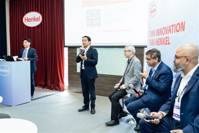
Mr. Kenji Kuriyama presenting at Henkel seminar and panel talk in SEMICON Taiwan 2025.
New Release: Loctite Eccobond LCM 1000AG-1 -Liquid Mold Material for Warpage Control in WLP and PLP Processes
Furthermore, as heterogeneous integration and photonic convergence become increasingly prevalent, advanced packaging technologies such as panel-level packaging (PLP) and co-packaged optics are gaining significant attention. PLP, for example, enables larger AI-enabling IC packages by improving scalability and manufacturing efficiency. However, these advancements introduce new challenges in managing the thermal demands of heterogeneously integrated devices-particularly in data center and smartphone applications-as well as in optimizing materials that interface directly with IC chips. A range of advanced materials-including liquid molded underfills (LMUF), first-level thermal interface materials (TIMs), and capillary underfills-are being developed to effectively distribute and extract heat, thereby enhancing device performance and reliability. Notably, the rise of advanced AI processors with stacked memory architectures has driven strong demand for molded underfill materials that address key challenges in 3D stacking and assembly, such as manufacturing throughput, process complexity, and overall cost.
Meanwhile, Henkel is introducing new innovations in fine-filler liquid compression molding (LCM) and molded underfill materials to support both near-term and long-term roadmaps for 2.5D and 3D packaging. These materials are designed to mitigate warpage while demonstrating excellent flowability and void-free filling capabilities at the wafer level, even in fine-pitch (<30 µm) and narrow-gap (<20 µm) configurations.
At SEMICON Taiwan 2025, Henkel launches Loctite Eccobond LCM 1000AG-1 , a new anhydride-free, ultra-low warpage liquid molding material designed for wafer-level packaging (WLP) and panel-level packaging (PLP) processes. This new product delivers stable warpage control throughout redistribution layer (RDL) processing, enabling high-yield, reliable advanced packaging solutions.
Working with Customers to Enable Materials for Next-Gen Semiconductor Devices
Advanced packaging is rapidly emerging as a key driver of innovation in semiconductor technology, enabling breakthroughs in system integration, performance, and sustainability. As an innovator in the advanced packaging materials space, Henkel is actively collaborating with Taiwan's leading industrial customers across critical areas-including new material design, customer support, green energy, and sustainable development.
This type of collaboration facilitates the sharing of knowledge, resources, and technology, accelerates global competitiveness, and ultimately achieves a win-win for more markets-helping to grow the global semiconductor industry. Henkel is committed to investing resources in solution design tailored to specific functions and maintaining long-term relationships with its customers.
Mr. Kuriyama shares two use cases that demonstrate strong momentum in customer collaborations in Taiwan. The first example is thermal cycle reliability for application processor chips. A customer approached Henkel to help pass thermal cycle reliability testing for an end customer's application processor. The challenge extended beyond reliability-it required enhanced processability for high-throughput production. Henkel responded by investing resources and developing new materials to meet the target and support the customer's goals.
Among the two cases, the second example focuses on underfill flow speed optimization. In this case, a customer was facing production bottlenecks due to the slow flow speed of their existing underfill material. Henkel stepped in to assess the specific requirements and engineered a faster-flowing underfill solution to replace the legacy product. This not only resolved the throughput issue but also significantly improved overall production efficiency. The case is well-articulated, outcome-driven, and demonstrates Henkel's ability to deliver tailored, high-performance solutions in advanced packaging.
The timelines for joint development projects vary significantly depending on the scope of work. Projects involving complex advancements-such as new process development or complete material replacement-can take two to three years. In contrast, initiatives focused on optimizing existing processes within current specifications are much faster, with development cycles of just three to six months.
In Taiwan, IC design houses, semiconductor foundries, and Outsourced Semiconductor Assembly and Test (OSAT) providers represent the three major customer types. Design houses focus on delivering new products with innovative IC chips, foundries explore novel materials for advanced packaging solutions, and OSATs emphasize manufacturing capabilities. Once a new material is introduced, Henkel's Taiwan-based application engineering and sales teams work closely with all customer types to ensure the material's functionality meets their specific requirements.
Henkel Provides Next-Level Support to Build Strategic Partnerships with Taiwan Customers
As semiconductor advanced packaging technologies continue to evolve, new opportunities are emerging across Co-Packaged Optics (CPO), panel-level packaging (PLP), and other next-generation formats. These innovations are reshaping how chips are integrated, aligned, and scaled for high-performance applications.
Taking CPO as an example, Mr. Kuriyama highlights it as a rising application in advanced semiconductor packaging. Henkel is developing light-pass adhesive materials to address the challenge of precise active alignment for optical components. These light-curing adhesives enable accurate alignment, supporting the assembly of complex optical systems within the CPO process.
Henkel Adhesives continues to invest heavily in material innovation and deepen its understanding of the evolving needs of the semiconductor and electronic materials markets. It is aligning its solutions with customers' technology roadmaps and contributing to the development of next-generation products. To fulfill these needs, the Henkel Taiwan Electronics Adhesives Technical Center in Zhubei City provides prompt technical support and fosters collaboration with Taiwan customers to accelerate prototyping and development. This Technical Center is dedicated to supporting innovation and product development through faster application simulation, data generation, and analysis—ultimately speeding up time-to-market for advanced packaging technologies.
As the industry shifts from a linear supply chain to a more integrated and collaborative ecosystem, Henkel Adhesives plans to strengthen its local support for Taiwan's semiconductor sector. This includes expanding beyond its application center by establishing local R&D resources and a satellite R&D office in Taiwan to provide direct, localized support. This strategic move will strengthen customer partnerships and accelerate the development of packaging technologies critical for AI chip innovation and the broader semiconductor ecosystem.
"Taiwan is a leading global center for advanced semiconductor process nodes and packaging innovations," Mr. Kuriyama concludes. "Through Henkel's dedicated support teams and close partnerships with customers, Henkel Adhesives is strongly committed to the Taiwan market and will contribute to technical breakthroughs that open a new frontier in advanced semiconductor packaging."
To learn more about Henkel and its advanced packaging solutions, visit the official Henkel website or official LinkedIn for more information.

