In late September 2025, three national governments enacted coordinated measures affecting Nexperia, a global semiconductor manufacturer recognized for its MOSFETs and small-signal discretes. The United States expanded export controls to include Wingtech Technology, Nexperia's parent company based in China. China introduced its own export restrictions impacting domestic manufacturing operations. Meanwhile, the Netherlands invoked the Goods Availability Act, resulting in the temporary suspension of the company's CEO and the transfer of shareholder voting rights to independent oversight.These combined actions significantly disrupted Nexperia's global production capacity, with nearly half of operations affected within days. Authorized distributors paused quotations, while brokers reported elevated pricing on remaining inventory. Buyers across the automotive, industrial, and consumer electronics sectors began urgently seeking alternative sources for critical components, with lead times extending into Q4 2025.This disruption was not the result of natural disasters or market-driven imbalances. Rather, it stemmed from a series of deliberate, cross-border regulatory interventions that had an immediate and substantial impact on commercial operations.Political Risk Now Comes From EverywhereThe Nexperia episode illustrates a fundamental shift in geopolitical risk. It no longer originates only in politically unstable regions but from the world's most advanced economies often concurrently. The United States, the European Union, and China are increasingly using trade policy, export controls, and corporate oversight as instruments of national strategy.This trend has been building. U.S. tariff policy shifted repeatedly throughout 2024 and 2025. Ocean freight rates from Shanghai to the U.S. rose 42% between December 2024 and January 2025. In August 2025, the U.S. implemented a 40% tariff on transshipped goods containing significant inputs from higher-tariff jurisdictions.For procurement teams, the assumption that stable trade corridors guarantee supply continuity is no longer valid. Risk is embedded in the structure of global commerce itself.The Nexperia Ripple EffectMajor contract manufacturers immediately assessed their exposure to Nexperia components. Regional responses varied. As highlighted by our recent article: Nexperia Supply Chain Update 2025, distributors in China halted quotations pending clarity on factory shipments. European distributors began segmenting inventory by country of origin to manage compliance exposure. In Asia, brokers reported active trading, accompanied by panic buying.Qualified alternatives from suppliers could not immediately absorb demand. Requalification cycles for automotive and industrial applications introduce delays that cascade into production stoppages. Even minor component shortages can trigger costly engineering reviews and line downtime.The New Normal of Government-Led DisruptionIn August 2025, global trade policy uncertainty reached 21 times its historical average surpassing even pandemic-era volatility. This is not a temporary anomaly. National security concerns, industrial policy, and strategic decoupling are driving sustained government intervention in commercial supply chains.Companies that continue to optimize solely for cost will face repeated disruptions. Those that embed resilience, transparency, and agility into their sourcing strategy will maintain operational continuity amid escalating uncertainty.The Nexperia event is not an outlier. It is a preview of a future where supply chains are treated as instruments of national interest and subject to sudden, coordinated intervention.Strategic Actions for Procurement Teams1. Diversify the supply base. Overreliance on a single supplier creates acute vulnerability, as demonstrated by the sudden unavailability of Nexperia components across multiple regions.2. Monitor early indicators of supply stress. Extended lead times, increased quote rejections, and pricing premiums, particularly for non-China-sourced parts, often signal tightening availability before formal shortages are announced.3. Cultivate executive-level supplier relationships. During allocation events, suppliers prioritize customers with established strategic partnerships, providing earlier visibility and preferential access to constrained inventory.4. Enhance supply chain transparency. Conduct comprehensive mapping of component exposure across all product lines to identify parts with limited alternatives or extended qualification cycles.5. Pre-qualify alternative sources. Waiting until allocation notices arrive places organizations at a significant disadvantage. Proactive evaluation of substitutes during design or routine reviews ensures readiness when disruptions occur.Secure Your Supply Chain Before the Next DisruptionWhen governments intervene or suppliers face sudden restrictions, having verified alternatives and real-time intelligence keeps your production running.Fusion Worldwide operates a global sourcing network with offices across North America, Europe, and Asia. Our e-commerce platform gives you 24/7 access to verified component inventory, transparent country-of-origin data, and alternative sourcing options when primary suppliers face constraints.Whether you need Nexperia alternatives, automotive-grade discretes, or hard-to-find components, our team provides the visibility and supply chain intelligence that helps you make confident decisions before shortages impact your bottom line.Visit www.fusionww.com to access real-time component availability and protect your production continuity.(Article written by Wei Liang Leu, Senior Director of Purchasing, APAC, Fusion Worldwide)
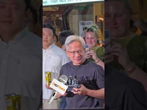
As artificial intelligence (AI) and semiconductors become central to the intensifying U.S.–China tech rivalry, and rare earth resource challenges elevate their strategic importance, the Office of National Assembly Member Song Seok-jun will host a high-level seminar titled "Global AI and Semiconductor Cooperation Strategy" on November 10, 2025 (Monday), from 9:30 AM to 11:30 AM at the National Assembly Library Grand Auditorium.The seminar will be co-hosted by Mr. Colley Hwang, Chairman of Taiwan's DIGITIMES Group, and Professor Sung Soo Eric Kim, Founder of Datacrunch Global, Adjunct Professor at Yonsei University Graduate School of Business, and Visiting Professor of AI Strategy at National Taiwan University.DIGITIMES is the world's largest semiconductor-focused media and research institution, co-founded by Morris Chang (Founder of TSMC) and Stan Shih (Founder of Acer). Chairman Colley Hwang is a globally recognized semiconductor strategist who has advised CEOs of leading ICT companies worldwide.Professor Eric Kim is a renowned authority in global AI strategy and a key figure in building semiconductor and AI cooperation networks across Korea, the United States, Japan, and Taiwan.This seminar marks a significant diplomatic and strategic occasion, with Taiwan's Ministry of Foreign Affairs dispatching an official envoy to participate. The event is expected to convene 300 attendees from government, industry, and academia to explore new pathways for international collaboration in emerging technologies.The event will take place on Monday, November 10, 2025, from 9:30 AM to 11:30 AM at the Grand Auditorium of the National Assembly Library, which accommodates up to 300 attendees. Registration is available via Google Form. For inquiries, please contact Professor Sung Soo (Eric) Kim.Korean National Assembly to Host Global AI and Semiconductor Cooperation Strategy Seminar. Credit: DIGITIMES
Dr. Ali Okhowat, a Canadian physician with a background spanning humanitarian work in conflict zones to co-founding the World Health Organization (WHO) Innovation Hub, is now using artificial intelligence to solve one of healthcare’s most persistent problems: administrative burden. Through his company Aya Health Technologies Inc., he has developed an AI scribe solution called "Autochart.ai Health Assistant". The team joins the Canadian Technology Accelerator for startups in the second half of 2025, leveraging Taiwan’s proactive push toward "smart hospitals" to enter Asian markets.Describing himself as "a physician by training, but a geek at heart," Dr. Okhowat's career trajectory is unique. After completing training in Canada, he worked with the International Committee of the Red Cross in low-resource and conflict areas, including Gaza and Afghanistan, followed by a post with the WHO overseeing the Middle East and North Africa. This field experience heavily influenced his belief in using technology to make care more accessible and efficient, eventually leading him to co-found the WHO Innovation Hub in Geneva.The Genesis of Autochart.ai Health AssistantThe concept for Autochart.ai was born from the direct experience of a practicing physician. Following his return to Canada and involvement in the COVID-19 response, Dr. Okhowat co-established a medical clinic in British Columbia intended to function as an innovation lab for digital health solutions.The resulting product, Autochart.ai, is an AI health assistant and clinical workflow solution designed to reduce the time health providers spend on documentation."The first part is that a note has to be generated documenting what actually happened and what the next steps were," Dr. Okhowat explained. "We are trying to help all health providers who are somewhat burdened with this task of having to create that initial clinical document, and then all of the downstream documents that are also needed, things like referral notes, patient communications messages."The solution, which is built on the Microsoft Azure Foundry and leverages various Large Language Models (LLMs), has been fully commercialized since November 2024 and is currently being used by subscribers in Canada and the US, including several British Columbia providers and health facilities involved in a provincial AI Scribe pilot program.A Focus on Multilingual ContextA key differentiator for Autochart.ai is its robust support for diverse linguistic environments. Recognizing the need for global utility, the company prioritized multilingual capability from the start."We translated the public-facing website fully into 10 different languages, and the interface into 13 different languages," Dr. Okhowat stated. "The number of languages that we accept in terms of input languages and output languages are over 100 different languages and dialects," including support for both simplified and traditional Chinese text. This focus aims to address not only single-language needs but also multilingual, multi-issue, and multi-patient encounters common in clinical settings. The software can also integrate visual context, such as analyzing images of dermatologic lesions, into the generated documentation.Scaling in Taiwan's Smart Hospital EcosystemDr. Okhowat's visit to Taiwan for the Startup Acceleration Program is timely, aligning with the government’s recent initiative to encourage hospitals to transform into "smart hospitals" by digital transformation, robotics, and AI.In response to Taiwan’s changing demographics and rising healthcare needs, the government has just launched the "Healthy Taiwan Deep Cultivation Plan" (2025–2029) in April with a total budget of NT$48.9 billion (US$1.63 billion), focusing on four key areas-better working conditions for medical staff, diverse talent cultivation, smart healthcare technology, and sustainable, socially responsible medicine-to advance tiered care, workforce retention, and healthcare system reform. Autochart.ai's strategy for entering the market centers on three pillars:1. Localization and Integration: Finding local partners to customize the solution and integrate it with Taiwan’s established Electronic Medical Records (EMRs) and world-class hardware manufacturers.2. Regulatory Adherence: Gaining a deep understanding of local data security and Taiwan FDA health pathway regulations to ensure full compliance. The system is already designed to support on-premise or local secure cloud environments to meet strict data privacy demands.3. Investment Synergy: Engaging with the local investor community to secure funding necessary for scaling the solution, with the goal of making it a "homegrown solution in Taiwan."The company offers flexible business models, including Software as a Service (SaaS), API-based integration, and licensing. Dr. Okhowat noted the potential for innovative monetization, moving toward a value-aligned model such as a per-chart fee with a managed upper cap to reduce costs for health systems.Future Vision: AI as a Total Health AssistantLooking ahead five years, the vision for Autochart.ai Health Assistant expands beyond supporting providers to directly empowering patients."We want to be able to help the patients just as much," Dr. Okhowat said. The company is currently developing a patient-facing AI scribe, voice agents, and physical AI implementations that would help individuals own and manage their medical records, make appointments, and summarize complex medical discussions for loved ones and their "circle of care." This evolution aims to transform the system into a comprehensive AI health assistant for all stakeholders, from providers to patients to health systems.Dr. Ali Okhowat
Ted Jin, founder and CEO of AuX Labs, is leading a charge in the food technology space with a mission driven by global impact and climate concerns. His company, which began operating around 2022, is pioneering the production of recombinant casein from yeast using precision fermentation to create animal-free dairy ingredients.Jin's journey into the bio-tech world comes after a decade in consumer packaged goods at companies like Procter & Gamble and PepsiCo, and prior experience in an earlier startup. His motivation isn't a personal dietary choice like being a vegetarian or vegan; rather, it's a deep-seated belief in the urgent need to solve food system challenges to sustainably feed a projected 10 billion people. "We aren't in a position that we can expand traditional animal agriculture," he stated, citing the finite nature of land and valuable resources.Precision Fermentation: A Non-Compromise AlternativeAuX Labs is focused on developing an ingredient: a casein powder that is functionally and nutritionally identical to the animal protein. This recombinant casein is produced by genetically manipulating yeast to express the protein. The goal is to provide a diversified protein source that doesn't force consumers to compromise on taste, function, price, or nutritional value.Jin sees their product as a necessary supplementation to-not a threat to-traditional animal agriculture. The company operates on a Business-to-Business (B2B) model, supplying this casein ingredient to consumer goods companies and food formulators to create end products like cheese.1. The Problem with "Wave One": Jin notes that the first wave of alternative proteins, which focused heavily on plant-based options, is subsiding as consumers demand products that are not just novel, but also taste good, are nutritious, and are priced comparably to animal products.2. Safety and Regulation: The company already holds a self-affirmed GRAS (Generally Recognized as Safe) status in the United States, which is crucial legwork in substantiating the protein's safety for human consumption.Global Expansion: A Look to Asia and TaiwanAuX Labs' core launch markets are currently Canada and the United States. The company is venture-backed, having closed a pre-seed and currently in the process of closing a new seed round, ensuring financial stability for the "coming period".Taiwan is positioned as the company's "first test" and a potential proving ground for Asian markets. Jin believes the Taiwanese market offers the agility of local companies and a population with a positive bias towards nutrition and health consciousness. A successful launch here would give the company confidence to pursue similar approaches in adjacent markets like Northeast and Southeast Asia (including Japan, Korea, and mainland China).Challenges to Overseas SuccessScaling into new markets is not without its difficulties, which Jin identifies in two key areas:1. Operating Expertise: Mastering the logistics of manufacturing in Canada and then exporting the casein ingredient into Taiwan, subject to the appropriate regulations.2. Local Partnerships: Finding a committed local partner in Taiwan, not just for the short term but for a multi-year effort. Jin stresses that this ingredient is novel, not just to Taiwan, but "new to the world".While the immediate plan is to import the Canadian-produced casein ingredient, establishing a local manufacturing presence in Taiwan remains an option if there is strong demand. Before that, the company will also need to validate their GRAS dossier and notify or file with the Taiwanese FDA.The Ultimate Goal: Price ParityJin's ultimate aspiration for AuX Labs is to be recognized as a pioneer in recombinant proteins. While he sees technology as "mature," he admits that the pricing is not mature yet. The final goal is to bring these animal-free proteins to market at a price point that is similar to animal proteins-something the regular consumer can afford-over the next few years. Achieving this price parity will be the key to establishing yeast-derived proteins as a viable and sufficient supply source for the global food system.Ted Jin, founder and CEO of AuX Labs. Credit: AuX Labs
Illumia Labs, a Canada-headquartered pioneer in Artificial Intelligence (AI) and Virtual Reality (VR) training, is targeting the Asia-Pacific market, with a specific focus on setting up a local presence and cultivating an advanced, AI-powered XR training ecosystem in Taiwan. The company, co-founded by two former Singapore Air Force pilots, is addressing a critical global labor shortage.Alan Tay, Illumia Labs co-founder and CEO, detailed the company's unique approach to immersive training with generative AI, their ambitious Series A funding plan and how the firm aims to leverage Taiwan's strong technological infrastructure in an interview with DIGITIMES.From Cockpit to Code: The Birth of a Digital HumanThe inspiration for Illumia Labs, according to Alan Tay, stemmed from a persistent real-world problem observed while running a flight school: a constant shortage of mechanics and flight instructors dating back to 2015, which significantly impacted the flight school's ability to produce trained pilots with reduced timeline.After successfully developing an initial Minimum Viable Product (MVP) in 2021 to digitize a flight instructor, the company began moving beyond aviation, realizing the potential for its technology across numerous vocations.Illumia Labs differentiates itself from traditional VR/AR training methods by focusing on human-centred AI. The core technology involves:1. Behavioural Replication: Training the AI to copy the human instructor's behaviour, subtle actions, and complex assessment methods using video data.2. Immersive Scenario-Based Learning: Placing the resulting "digital human" into immersive environments (VR, AR, or XR) where it can act as a mentor or role-playing partner.3. Sensor Agnosticism: The technology is not restricted to bulky goggles but can be integrated into AR/XR glasses or sensor-filled training rooms."We are not there to replace the human, but to make sure that the human is capable doing their jobs with much more proficiency," Tay stated.Beyond Maintenance: AI in Customer ServiceWhile founded in aviation and mechanics, the company has found diverse applications for its technology, particularly in customer service such as training flight attendants, banking staff and other customer facing staff. The AI is designed to ensure a "gold standard" of service that includes proper tone, language, and body language.A key unique feature is the AI's ability to conduct evaluation while the trainee is physically performing a task. For example, the AI can role-play as a "disruptive passenger" while a flight attendant trainee practices virtual food service in a confined space. This hands-on, contextual assessment offers a dynamic and individualized immersive training experience unlike simple chatbot conversations.Crucially, the system is designed to handle multilingual and culturally sensitive training.Alan Tay noted that the product is designed to be 80% complete, stating: "The other 20% I need the local experts to let us know what are the local customs. We can add on, and our AI learns from the video." This final, customized portion is built into the business model as a one-time Non-Recurring Engineering (NRE) fee, alongside standard SaaS licenses and seed models for larger organizations.Aggressive Expansion and Taiwan's RoleIllumia Labs is executing an aggressive scaling plan, following its successful model in Singapore and a recent expansion into Malaysia. Participating in the CTA program, the company views Taiwan as a strategic hub for the Indo-Pacific rollout.The biggest challenge the company faces is not technological capability, but infrastructure and data connectivity. "Not everywhere has accessibility to 5G," Alan Tay lamented, citing issues with latency and computing power accessibility in various global markets. However, the co-founder expressed optimism about Taiwan, stating that its advanced infrastructure is expected to make the local rollout "a lot more smoother" than in other parts of the regions. "Taiwan's success stories", he added, "will serve as vital pilot cases for further international scaling."Alan Tay, founder of Illumia Labs. Credit: Illumia Labs
Anandi Botanicals Inc., an Alberta-based startup, is pioneering sustainable, high-tech agriculture by merging advanced plant biotechnology with AI and robotics. The company seeks research and commercial partnerships in Taiwan to scale its solutions for high-value crops and enhance global food security.The company specializes in plant tissue culture and AI-driven optimization across agriculture, horticulture, forestry, and conservation. Founder and Technical Director Dr. Annie Ray, a plant biologist with over a decade of international experience, established Anandi Botanicals in 2024 to address limitations in traditional propagation methods. "Seeds in seed banks often degrade, are susceptible to infection, and may not survive," she explains, making tissue culture "almost the only option" for rare and endangered species.Dev, Co-founder and Chief AI Officer, brings over 20 years of expertise in product development, AI, and automation. The founders' complementary backgrounds allow the company to scale tissue culture efficiently, automating labor-intensive processes that become unviable at large volumes.The process begins with explants from certified mother plants and follows stages including callus induction, shooting, rooting, acclimatization, and greenhouse hardening. The result: virus-free, disease-free, uniform plants with faster growth and scalable production. Techniques include protoplast culture and microfluidics, with AI models analyzing data to optimize workflows and reduce research time. Local GPU execution ensures data privacy, while IP-protected logistics solutions maintain plant viability during shipping, reducing damage from 70–80% in traditional transport.Taiwan Market and Global StrategyThrough the Canadian Technology Accelerator, Anandi Botanicals seeks Taiwanese partners for both R&D and commercial production. Target crops include orchids, pineapples, mangoes, asparagus, garlic, and medicinal plants. Partnerships with universities, biotech parks, and local nurseries will support technology adoption and automation integration.The company is leading research on perennial grains in collaboration with the NRC. Perennial grains do not need to be seeded every year, staying in the ground for at least three years. This improves soil quality by increasing carbon content and aeration and requires less tilling.On the research front, the company collaborates with Canada's National Research Council on perennial grains, which improve soil quality, reduce tilling, and provide multi-year yields. A proposal has been submitted to the UN FAO as a global food security solution. Taiwan's focus on sustainability and high food import reliance makes this technology highly relevant.Business Model and Future OutlookAnandi Botanicals operates a dual model: direct sales for crops without IP restrictions and licensed production for valuable IP-protected crops, offering royalties or licensing options. Its AI and automation technologies are being patented, with collaborative sharing possible under NDAs.For their technologies, including their AI-related solutions and workflow automation, they are in the process of IP registration. They are open to the transfer and distribution of their AI technologies through agreements like mandatory NDAs, emphasizing that this is crucial for global food security. Importantly, they are willing to negotiate IP terms and are "more than agreeable to discuss those opportunities" when collaborating with government establishments for the betterment of the entire community or country.Over the next five years, Anandi Botanicals aims to lead the integration of AI, robotics, and biotechnology in agriculture, increasing efficiency in production and research. By partnering with global institutions, governments, and commercial entities, the company seeks to scale field trials, expand perennial crop production, and contribute to global food security.Founder and Technical Director Dr. Annie Ray, Anandi Botanicals.
The robotics sector is booming, yet a fundamental challenge persists: moving autonomous machines safely and efficiently from the controlled environment of a warehouse into the complex, unpredictable flow of daily life. Vancouver-based startup Ma Robot AI is tackling this issue head-on with its specialized "Embodied AI" software, designed to grant robots and autonomous vehicles human-level intuition in dense, high-traffic areas.Founded by a unique partnership, Ma Robot AI is led by CEO Winnie Liang, who brings a background in business and workflow automation from her time at PriceWaterhouseCoopers (PwC), and CTO Dr. Mo Chen, a distinguished authority in the field as a Canadian Institute for Advanced Research (CIFAR) AI Chair and Computer Science faculty member at Simon Fraser University, with a recent visiting professorship at Stanford. They are co-founder husband and wife. The need for their combined expertise emerged during the pandemic, as they witnessed how overwhelmed hospital staff spent crucial time on manual, repeatable delivery tasks.The Technology: Intuition Without DataMa Robot AI's core offering is a patent-pending hybrid AI system that fundamentally shifts how robots perceive and interact with uncontrolled environments. Unlike conventional solutions that rely on extensive data collection for specific environments (a key bottleneck for scaling), Ma Robot AI's software operates in real-time, on the edge, and requires no prior data from the target location.The critical differentiator is the concept of "interpretable AI," which allows robots to predict how human agents will move in time and space, enabling them to navigate safely and confidently among people. This technology is applicable not just to delivery robots, but also to autonomous and computer-assisted driving systems, offering potential improvements in safety and efficiency on urban streets.Scaling Strategy: From Integrator to LicensorHaving incorporated nearly two years ago, Ma Robot AI, currently a team of eight, is pursuing a two-phase business model. Initially, the company acts as a system integrator (SI), pairing its software with cost-efficient, high-performance third-party hardware (often sourced from Asia). This approach is currently being piloted in a BC hospital, where a robot is helping deliver lab samples-a project supported by a grant from the BC government.The long-term vision is to transition entirely into a software licensing model. By showcasing the power of their AI through successful pilots, the company aims to establish trust with major global hardware vendors. This would allow manufacturers to license Ma Robot AI's software to upgrade their own mobile robots and vehicles, significantly accelerating market entry into high-impact sectors like healthcare and urban logistics.Liang emphasized that Ma Robot AI will focus on AI algorithms and software, which is their core strengths, and refrain from producing robots themselves.Eye on the Asia-Pacific MarketMA Robot AI is leveraging a Canadian Technology Accelerator (CTA) program to focus its international expansion on Taiwan's technology and manufacturing ecosystem. CEO Winnie Liang emphasized that Taiwan's strength in hardware, robotics, and supply chain efficiency makes it a perfect partner to scale their software-centric product.The company is actively seeking strategic partnerships with local industry leaders, technology integrators, and investors, with specific interest in meeting groups like URS Robot, Turin Drive, and Kingswaytek Technology during its November visit.Ma Robot AI is targeting an early-next-year Seed Funding Round, aiming to capitalize on the traction generated by their pilot successes and solidify their transition from a startup with promising technology to a pivotal software licensor in the global robotics landscape. Their ultimate goal is to see their AI bring robots out of the industrial warehouse and into broad, collaborative use alongside the human workforce within the next five years.Winnie Liang, CEO of Ma Robot AI. Credit: Ma Robot AI
Wireless PnC, a cleantech company based in Victoria, British Columbia, is making waves in the micromobility sector with its highly efficient and universally compatible wireless charging technology. The company, founded by Dr. Samira Soltani, aims to streamline fleet operations, reduce emissions, and accelerate the adoption of sustainable transportation globally.In an exclusive interview, Ishtdeep Singh, the company's Product Development Head, detailed the technology, the company's strategic focus on the Asian market, and current funding efforts.The Universal Charging SolutionThe inspiration for Wireless PnC came from the growing need for convenient, efficient, and standardized charging for light electric vehicles, particularly e-bikes and e-scooters."The current plug-in charging technology is not able to solve the universality issue," explained Singh. "Some are compatible only with bikes, some only with scooters. With our single wireless charging pad, it is universal among different kinds of vehicles, whether it is an e-bike, an e-scooter, or even an industry robotic vehicle."The system relies on inductive charging, comprising two parts: a receiver module mounted on the vehicle (e-bike/e-scooter) and a ground pad connected to a standard 120-volt wall plug. This simple infrastructure is a major differentiator, requiring minimal footprint and zero large-scale upgrades or vehicle redesigns.A Leap in Efficiency:Wireless PnC claims a significant technological advantage in power transfer efficiency. While traditional plug-in solutions operate at 85% to 88% efficiency, Wireless PnC achieves an impressive 95% efficiency, with only a minimal 5% power loss. This reduces power consumption by up to 30% compared to other chargers and translates to more than 400 W-hrs saved per charge for larger e-bikes-a significant benefit over the vehicle's lifetime.This is attributed to patented coil designs and a novel shielding mechanism.Furthermore, the system is designed for low maintenance and durability, having been successfully tested outdoors on concrete pads in rain and snowy conditions.Asia-Pacific Strategy: Leveraging Taiwan's EcosystemWith the e-scooter and e-bike culture booming across North America and Asia, Wireless PnC views the Asia-Pacific region as a critical market. The company is actively seeking to leverage Taiwan's strong manufacturing and semiconductor ecosystem.The company is looking for Taiwanese partners to build key hardware components, including PCBs, charging coils, and communication chips (like Wi-Fi ESP chips).Singh confirmed that the current visit to Taipei is about more than just supply chain. Wireless PnC is actively seeking a strategic investment to use Taiwan as a "bridge" to enter the broader Asian market, including major hubs for light electric vehicles like India and Malaysia. While the initial focus is on e-scooters and e-bikes, the company sees potential expansion into three-wheelers, golf carts, and e-rickshaws.Company Status and FundraisingWireless PnC was officially incorporated in 2023, though the idea was initiated by co-founders Dr. Samira Soltani (CEO) and Dr. Sahar Sam (Serial Entrepreneur) back in 2020. Headquartered in Victoria, British Columbia, the company currently employs 14 full-time staff.The company has completed indoor testing and MVPs and has already tested its technology with two prominent bike-sharing companies in Canada. An outdoor pilot installation is planned for the near future at an educational institution in Canada.Wireless PnC is currently seeking to raise US$1 million in a pre-seed funding round. These funds are earmarked for product development, pilot installations, team expansion, and securing additional non-dilutive grants, all aimed at scaling wireless charging stations and strengthening partnerships with fleet operators and municipalities. The company has already successfully secured nearly US$1 million in non-dilutive funding through grants and subsidies.Wireless PnC is positioning itself as a leader in the cleantech transition, offering a versatile charging solution that could become a key infrastructure component for smart cities worldwide.Wireless PnC CEO and Fouder, Dr. Samira Soltani. Credit: Wireless PnC
MaxEpic, a nascent but rapidly advancing chiplet semiconductor startup based in Canada, is spearheading the development of next-generation fully-integrated power delivery and power integrity solutions crucial for the escalating demands of AI systems.Founder and CEO Dr. Jerry Zhai is a seasoned veteran who has accumulated over two decades of experience in semiconductor technologies, product development, and business development with companies such as Analog Devices, Samsung Semiconductor and Renesas."AI has made a tremendous inroad in our industry from component to system level. The technology we have developed is a highly integrated power delivery chiplet that can address the new and rigorous demand of AI systems," said Zhai. "That is a fundamental force which drove us to start up this company."The company, which began its focused development just about two years ago, is moving swiftly. Already, the company has successfully engaged with multiple major AI industry players, including large-scale hyperscalers, AI machine makers, semiconductor companies, and manufacturing partners, underscoring the immediate industry relevance of their solution.Addressing the AI Power and Thermal CrisisThe dramatic advancements in AI hardware, such as GPUs, CPUs, and High Bandwidth Memory (HBM), have resulted in an unprecedented power dilemma. Dr. Zhai points out that the electrical current drawn by these components has increased three to five times over prior generations.Modern CPUs, for instance, can consume up to 1,000 Amperes at a very low voltage of around 0.7 volts. The voltage for HBM continues todecrease. For example, the I/O voltage is down to 0.4V now to meet the low latency and high speed of data transmitting. The layer stack up of HBM that has increased up to 12 layers to meet workload demands has raised the HBM current consumption and density dramatically. This extreme current level and super high density create immense systemic challenges, including thermal dissipation issues and limits on I/O ports.MaxEpic's innovative power delivery method trademarked as Ivy-ChipletTM is a fundamental solution to this challenge. It utilizes a proprietary IP to perform high-efficiency voltage conversion. Instead of drawing 0.7 volts directly, the device can effectively take a voltage that is twice or three times higher, such as 1.4 volts or 2.1 volts. In HBM I/O power which needs 0.4V, the voltage converstion ratio is 5-to-1 or 6-to-1 and the input voltage become 2.0V or 2.4V As a consequence of this voltage conversion, the current flowing into the device is instantly reduced by half, two-thirds or even less, depending on the designed voltage conversion . This significant reduction in current directly alleviates the problems of I/O port limit and thermal challengess by dramatically reducing power loss along the delivery path. The efficiency of MaxEpic's technology is remarkable, achieving up to 97% with its proprietary power streaming circuitsTechnological Edge and Versatile ApplicationsThe Chiplet's design offers significant flexibility in integration. It can be used as a standalone device or be seamlessly integrated directly into the AI device's package using contemporary 3D packaging technology.MaxEpic's device is implemented using FinFET nodes, designed to be fully compatible with more advanced nodes like 7 nanometer, 5 nanometer, or even lower. This compatibility with cutting-edge process technology is vital, as the more advanced a chip is, the more efficient its power management needs to be.The high efficiency, excellent thermal properties, and dimensional profile of MaxEpic's solution expand its potential beyond high-performance computing (HPC) and data centers. The technology can address systems requiring high degrees of integration and size reduction in three dimensions. Potential applications include next-generation AI glasses, which have a huge demand for high integration, small size and low profile, and Electric Vehicle (EV) systems, which benefit from the high reliability the technology offers.Founder and CEO Dr. Jerry Zhai, MaxEpic. Credit: MaxEpic
In an era defined by increasing volatility from climate change and complex infrastructure challenges, Canadian 6D simulation firm RUNWITHIT Synthetics is pioneering a novel approach to urban resilience. The company, a Certified Indigenous and women-led enterprise based in Edmonton, is building " live 6D AI-driven models of cities and regions" using its proprietary 6D simulation generative AI platforms.Myrna Bittner, Founder and CEO of RUNWITHIT Synthetics, describes the company's core mission as bridging the "critical gap between very complex data and real human experience." The goal is to make data accessible, enjoyable, and relevant for leaders-many of whom are not technologists-who are making critical policy and investment decisions around resilience, new energy technologies, and community welfare.The Power of the Living Digital TwinRUNWITHIT Synthetics does not rely solely on existing historical data, a significant differentiator in a field often constrained by data availability. Instead, their technology is built to thrive in scenarios where historical data is scarce or where anticipated events-like an extraordinary cold snap in a warm city-have never occurred."We shouldn't let data be our barrier when we need to be looking and planning in the future," Bittner states.The company's platform consumes diverse inputs-from spatial and satellite data to public census and research-to synthesize a "living form of reality." It then runs "superscalar simulations" on this digital twin, generating new, reliable data from configured, novel scenarios through emergent behavior modeling.This approach requires a highly diverse team, blending deep-tech social system engineers, AI programmers, game engine developers, designers, and animators. The inclusion of design is deliberate; as Bittner notes, making the future compelling and beautiful makes data more accessible.Furthermore, the company is highly focused on efficiency, utilizing clustering technology, parallel processing, and federated generative AI to minimize computing consumption, allowing complex simulations to be run even on a laptop.Versatility: Driving Strategic Decisions Across Multiple ScenariosThe power of RUNWITHIT Synthetics' platform lies in its modular and adaptable architecture, which allows customers to flexibly integrate modules for distinct strategic purposes. Applications span beyond disaster management to include long-term strategic advisory, community growth planning, and infrastructure design."Customers can choose a focus area and not even be limited by that one focus area," Bittner explains. The platform enables users to model the intricate connections between design response, energy resilience, public health, social infrastructure planning, and security environments. This interconnectedness allows clients to effectively navigate the comprehensive impact of various decisions on the built environment, the natural environment, and the community.Globally, the company is tackling major challenges such as modeling the impacts of extreme cold in Nashville and working with the Government of Canada to improve resilience in rural communities. This Canadian project, for example, models the interconnections between energy, health, and communication systems while assessing the benefits of implementing distributed energy resources like solar, wind, and virtual power.Asia Expansion: Applying Versatile Planning Tools in TaiwanA major focus for the company is market expansion, with Taiwan serving as a key strategic access point for Southeast Asia. The recent Hualien flood disaster provided a stark reminder of the challenges the region faces.In light of this, RUNWITHIT Synthetics has already established foundational relationships, notably with the Taiwan Indigenous Sustainable Development Association and the Council of Indigenous Peoples (TISDA). Their goal of joining the Canadian Technology Accelerator (CTA) program is to advance digital twin applications for rural and indigenous communities in Taiwan, focusing on emergency preparedness, improved health access, and sustainable energy development-precisely the kind of interlinked systems analysis needed for planning and disaster recovery. They are also seeking to reinvigorate conversations with the National Health Research Institutes (NHRI) regarding health research simulations involving population data, which is crucial for managing health crises following a natural event.Myrna Bittner, Founder and CEO of RUNWITHIT Synthetics. Credit: RUNWITHIT Synthetics