

SK hynix Inc. announced today that it has completed development of its 321-layer 2Tb QLC NAND flash product and has begun mass production. This achievement marks the world’s first implementation of more than 300 layers using QLC technology, setting a new benchmark in NAND density. The company plans to release the product in the first half of next year following completion of global customer validation.
1NAND flash is categorized as single-level cell (SLC), multi-level cell (MLC), triple-level cell (TLC), QLC, and penta-level cell (PLC) depending on how many data bits can be stored in one cell. As the amount of information storage increases, more data can be stored in the same volume.
To maximize the cost competitiveness of its new product, SK hynix developed a 2Tb device with double the capacity of existing solutions. To address potential performance degradation in large-capacity NAND, the company increased the number of planes, independent operation units within a chip, from 4 to 6. This enables greater parallel processing and significantly enhances simultaneous read performance.
2A plane refers to a cell and its peripheral circuitry that can operate independently within a single chip. By increasing the number of planes from 4 to 6, the simultaneous read performance of the chip—a key factor in data processing—is significantly improved.
As a result, the 321-layer QLC NAND delivers both higher capacity and improved performance compared to previous QLC products. Data transfer speed has doubled, write performance has improved by up to 56%, and read performance has improved by 18%. In addition, write power efficiency has increased by more than 23%, strengthening competitiveness in AI data centers where low power consumption is critical.
The company plans to apply its 321-layer NAND first to PC SSDs, before expanding to enterprise SSDs (eSSD) for data centers and UFS for smartphones. Leveraging its proprietary 32DP3 technology, which enables the simultaneous stacking of 32 NAND dies in a single package, SK hynix aims to enter the ultra-high-capacity eSSD market for AI servers by achieving twice the integration density.
332DP (32 Die Package): A method of simultaneously packaging 32 dies in one package to increase chip capacity.
“With the start of mass production, we have significantly strengthened our high-capacity product portfolio and secured cost competitiveness,” said Jeong Woopyo, Head of NAND Development at SK hynix. “We will make a major leap forward as a full-stack AI memory provider, in line with the explosive growth in AI demand and high-performance requirements in the data center market.”

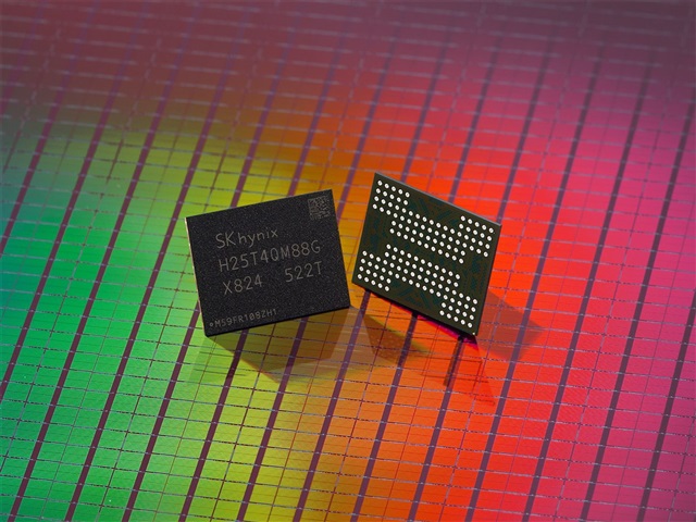
SK hynix begins mass production of the world’s first 321-layer QLC NAND flash chip with 2Tb capacity. SK hynix
