
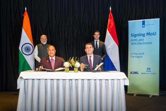
Tata Electronics has signed a memorandum of understanding with ASML to support the establishment and ramp-up of its upcoming 300mm semiconductor fab in Dholera, Gujarat, marking a significant step in India's effort to build a domestic chip manufacturing ecosystem.
The partnership will see ASML provide lithography tools and related solutions for Tata Electronics' Dholera fab. The companies said the collaboration will also cover talent development, lithography-related skill building, supply chain resilience, and R&D infrastructure.
Lithography is one of the most critical and complex steps in semiconductor manufacturing. ASML's involvement is therefore significant for Tata Electronics as it attempts to move India's semiconductor ambitions from policy-backed announcements toward commercial-scale execution.
Tata Electronics is developing the Dholera facility as India's first commercial 300mm semiconductor fab. The project carries a planned total investment of US$11 billion and is expected to manufacture chips for automotive, mobile devices, AI, and other applications.
The company has already partnered with Powerchip Semiconductor Manufacturing Corporation (PSMC) of Taiwan for technology support. Through that partnership, Tata Electronics has access to a process technology portfolio covering 28nm, 40nm, 55nm, 90nm, and 110nm.
These nodes are typically associated with mature and specialty applications rather than leading-edge logic, but they remain widely used across automotive, industrial, power management, connectivity, and mixed-signal markets.
The ASML agreement adds another important piece to Tata's semiconductor roadmap, particularly on the equipment and process side. Tata Electronics said construction of the fab is progressing rapidly.
Dr Randhir Thakur, CEO and managing director of Tata Electronics, said ASML's lithography expertise would support the timely ramp-up of the Dholera fab, help create a trusted supply chain for global customers, and support local talent development.
ASML CEO Christophe Fouquet said the company sees long-term opportunities in India's expanding semiconductor sector and expects to work closely with Tata Electronics and its broader ecosystem.
The companies framed the partnership as part of broader strategic cooperation between India and the Netherlands in critical technologies, including semiconductors.
India's semiconductor industry body also welcomed the agreement. In a statement, Ashok Chandak, president of IESA and SEMI India, called the Tata-ASML partnership a "breakthrough and a historic milestone" in India's semiconductor manufacturing journey.
For India, the deal comes at a time when the country is trying to position itself as an additional semiconductor manufacturing location amid global supply chain diversification. While India has a strong chip design base, it has so far lacked commercial-scale wafer fabrication capacity.
The Tata-PSMC fab in Dholera is central to the country's manufacturing ambitions. However, building a fab requires not only capital expenditure and technology licensing, but also access to highly specialized equipment, process expertise, trained engineers, and a reliable supplier base.
The ASML partnership signals that Tata Electronics is moving to deepen relationships across the semiconductor value chain. For ASML, the MoU deepens its engagement with India's emerging semiconductor manufacturing ecosystem.
Operational reality beyond the symbolism
Chandak said India's semiconductor momentum is now moving "from vision to execution and outcome." For industry observers, the key question will be whether partnerships such as Tata-ASML can shorten India's learning curve in wafer fabrication and help the country build a credible role in the global semiconductor supply chain.
Sanchit Vir Gogia, chief analyst and CEO at Greyhound Research, said the significance of the Tata-ASML partnership lies less in national symbolism and more in whether Tata can build a manufacturing system that global semiconductor customers can eventually trust.
"ASML de-risks the lithography layer. It does not de-risk the fab," Gogia said. The harder question, he added, is whether Tata can institutionalize yield learning, supplier discipline, and customer qualification faster than India's supporting ecosystem matures.
Gogia cautioned against reading the ASML partnership as a sign that India is entering leading-edge semiconductor manufacturing. He said there is no credible basis for assuming the Dholera fab is an EUV-driven project. A more realistic interpretation, he said, is that ASML's role points to a DUV-led mature-node and specialty semiconductor manufacturing stack.
According to Gogia, this is still commercially significant because mature-node semiconductors remain critical for automotive, industrial, telecom, medical, energy infrastructure, sensors, analog, mixed-signal, and power management applications.
He said Tata's broader semiconductor positioning also matters, with PSMC supporting process transfer, ASML supporting lithography, and Tata's Assam OSAT project adding downstream packaging and test capability. However, he said India still faces gaps in process-engineering depth, supplier ecosystems, semiconductor-grade chemicals and materials, yield engineering talent, and equipment maintenance infrastructure.
Gogia said the credible marker for commercial operations is around FY2029-30, assuming construction, tool installation, process transfer, qualification, utilities readiness, and yield learning remain broadly on track. "A wafer can be produced before a fab becomes dependable," he said.
Article edited by Jack Wu