As AI models and computing demands continue to grow exponentially, the biggest challenge in chip design is no longer pure processing power, but the bandwidth gap between processors and memory. Even with continuous improvements in processor performance, if data cannot be delivered in real time, overall system efficiency remains limited.
To overcome this bottleneck, Die-to-Die high-speed interconnect and HBM4/PHY IP integration have emerged as critical technologies for next-generation AI and HPC chip designs.
Progate Group Corporation(PGC), a member of the TSMC Design Center Alliance (DCA), leverages its ASIC turnkey expertise and participation in the Synopsys IP OEM Program to deliver advanced design capabilities comparable to leading international players-while offering a more cost-effective, high-value service model that helps global customers accelerate AI and HPC deployment and mass production.
Technical Highlights: Comprehensive Support from Design to Production
PGC provides one-stop technical services, supporting clients from chip design to production. The coverage includes high-speed interconnects, memory integration, foundry certifications, and AI/HPC application-oriented designs, helping clients shorten time-to-market efficiently.
Die-to-Die Interconnect and Chiplet Architecture
PGC offers advanced expertise in Die-to-Die interconnect and Chiplet-based system design, supporting 2.5D and 3D integration technologies to enable high-speed, low-latency, and low-power chip-to-chip communication. All solutions are compliant with the Universal Chiplet Interconnect Express (UCIe) standard, ensuring interoperability and scalability across heterogeneous and cross-supply-chain environments.
This capability addresses the growing demand for high-bandwidth and flexible multi-die integration, empowering customers to build next-generation Chiplet-based systems with enhanced performance and modularity.
HBM4 / PHY IP Integration
Leveraging Synopsys-certified IP, PGC enables rapid integration of HBM4 memory and PHY interfaces to shorten design cycles while strengthening design reliability. These high-bandwidth memory solutions help design teams overcome data transfer bottlenecks and achieve terabyte-per-second (TB/s) throughput, meeting the stringent performance requirements of AI and high-performance computing (HPC) applications.
TSMC DCA Certification Advantage
As a certified member of TSMC's Design Center Alliance (DCA), PGC provides end-to-end design-to-tape-out support within the TSMC's ecosystem. Customers can leverage TSMC's CyberShuttle multi-project wafer (MPW) program to conduct rapid prototyping and design validation, followed by seamless transition to mass production through PGC's ASIC turnkey services. All designs are fully compatible with advanced packaging technologies such as Wafer-on-Wafer (WoW) and 2.5D/3D integration architectures within major foundry ecosystems, ensuring a smooth and efficient path from prototype to production.
AI / HPC Application Focus
PGC's dedicated ASIC designs are optimized for AI and high-performance computing (HPC) applications, spanning AI accelerators, data center chips, and high-speed network switch devices. These designs support AI training, HPC simulation, and large-scale data processing workloads, meeting the performance, power, and scalability requirements of next-generation computing environments.
Ecosystem Integration
PGC's services are closely aligned with TSMC's advanced foundry ecosystem, combined with Synopsys-certified EDA and IP solutions, to deliver a complete ASIC turnkey flow covering: High-speed interface IP - ASIC design service - process support - packaging service - verification - testing - mass production.
In addition to its own testing equipment and validation capabilities, PGC maintains long-term partnerships with multiple advanced test houses, enabling precise analysis for high-frequency, high-speed interface and advanced-node devices.
This level of integration significantly reduces design risk and accelerates time-to-market, while ensuring that the design results are fully compatible with mainstream advanced packaging technologies - such as 2.5D/3D integration and wafer-on-wafer architectures within major foundry ecosystems - as well as international standards including UCIe.
PGC delivers high reliability, low risk, and accelerated time-to-production through its comprehensive ASIC turnkey services, allowing customers to focus on differentiated design and market innovation. By leveraging its proven engineering expertise and established partnerships across the semiconductor supply chain, PGC helps customers reduce overall design and ASIC development costs, enhance design success rates, and improve product stability.
In addition, PGC provides cross-regional engineering and project management support spanning Taiwan, Japan, China, and the United States - empowering global deployment strategies for AI and HPC applications with consistent quality and technical alignment.

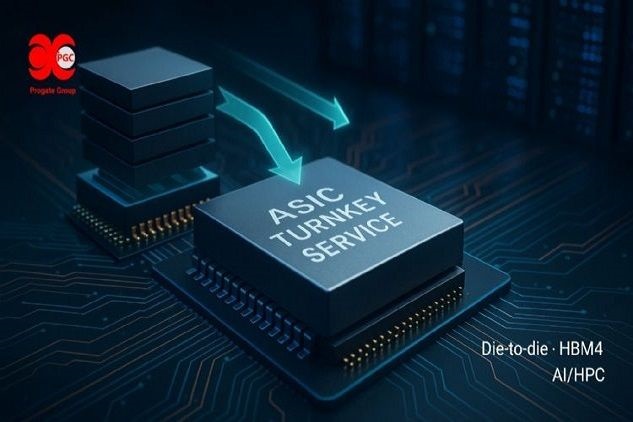
PGC provides complete ASIC turnkey services supporting 2.5D/3D advanced packaging technologies.Credit:PGC