

Huawei has confirmed in a posting on its website reports about its breakthrough in making a light source component used in EUV lithography systems which are required for making high-end processors on sub-10 nm nodes.
The Chinese tech giant posted a video on its website to back claims about its EUV lithography breakthrough. It also claimed to have "entered the game" on its official website.
China tech news media MyDrivers quoted China's National Intellectual Properties Administration website information saying that Huawei Technology filed an application for a patent covering a EUV lithography process and its key components in mid-November. The patent application number is 202110524685X.
Huawei's application has not been approved yet. It is difficult to judge whether Huawei already has the ability to produce the entire EUV equipment.
Huawei said on its website the latest patent application shows the usage of EUV lithography technology to improve the manufacturing of integrated circuits and chipsets.
"Together, this process will form an interference pattern that will keep on changing with new light rays. Consequently, this will equalize the light exposure and will solve the un-uniform light issues that often occur in chip development," according to Huawei's website description.
Alongside uniform light rays, this mechanism will ease the creation and formation of the nano-particles that are assembled in the integrated circuits or the micro-chipsets.
"Further, lithography mainly performs the transfer, processing, and creation of micro-nano graphics. It also verifies the total elements equipped in a chipset and checks the appropriate size and other details in the circuits," according to Huawei.
A UDN report said in addition to Huawei, local research institutions in China, such as Tsinghua, have also put forward EUV lithography-related technologies to overcome the light source technology barriers, mastering new light sources that can be used for EUV lithography. The Chinese Academy of Sciences also mastered the mirror system technology.
Despite the breakthrough in EUV light source technology, the EUV machine is not easy to manufacture, because there are more than 100,000 components in a EUV machine, requiring the collaboration of a huge supply chain, which is a major obstacle for any country trying to build the equipment from scratch without getting help from other component sources.
Huawei has been quietly developing a domestic semiconductor ecosystem over the past few years trying to counter the US tech export sanctions that have kept it from accessing advanced chips. It has invested in a wide range of companies in the semiconductor supply chain, starting from EDA, equipment, and materials, to foundry, testing, and packaging.
The technology for which Huawei is applying for a patent is trying to solve the problem of uneven light intensity of the light source used in the EUV lithography machine. According to the disclosed information, the patent application provides a reflector, a lithography device, and a control method thereof, which relates to the field of optics and can solve the problem that coherent light cannot be homogenized due to the formation of a fixed interference pattern and is optimized on the basis of the lithography device for extreme ultraviolet light, thus achieving the purpose of homogenization.
The UDN report said while Huawei is developing EUV lithography, it is also developing technologies that "bypass" lithography. For example, it is bypassing the US monopoly technology of silicon wafers in favor of optoelectronic wafers and other practices.
Interestingly, ASML, the company which is the sole provider of EUV equipment in the world, applied for a similar patent (US2016007434A1) in 2016 but has a different scope of patent rights.
The difference between the two patents is that Huawei uses a rotating illumination device to reduce the number of bright or dark patterns in the same area, while ASML's patent allows the same beam of light to be split and incident at different points to produce a uniform light on the relative movable and stationary flat panels and reflector sets.
ASML's EUV machine uses Cymer's light source device. Cymer is headquartered in San Diego, California, and was acquired by ASML in 2013.
It took ASML 17 years to develop the first-generation multi-patterning EUV equipment, which has been used only by TSMC, Samsung, Micron, Intel, and SK Hynix so far. Currently, China is prohibited from accessing EUVs, but is able to import DUVs which are used to produce mature node chips of 28nm and above.
According to ASML's website, its EUV technology uses light with a wavelength of 13.5nm, which is more than 14 times shorter than DUV light.
The laser-produced plasma (LPP) source, molten tin droplets of around 25 microns in diameter are ejected from a generator at 70 meters per second. As they fall, the droplets are hit first by a low-intensity laser pulse that flattens them into a pancake shape. Then a more powerful laser pulse vaporizes the flattened droplet to create a plasma that emits EUV light. To produce enough light to manufacture microchips, this process is repeated 50,000 times every second.
ASML has announced in its third-quarter 2022 earnings conference call that it will continue to ship DUV lithography equipment to China and that it will increase its production capacity to 90 EUV and 600 DUV systems (2025-2026) and increase its High-NA EUV capacity to 20 systems (2027-2028).
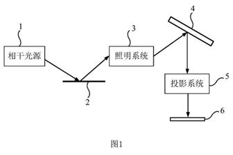
Diagram 1 in Huawei's patent application 202110524685X. Source: CNIPA
Photo: CNIPA