The recent global shortage of automotive chips has brought Taiwan's semiconductor industry into the focus of worldwide attention. The real cause of why Taiwan's semiconductor chips are in such great demand is due to their trusted, unwavering quality that's supported and assured by a series of rigorous verification procedures. The electrical measurement performed before integrated circuit packaging is one of the most important steps of verification. To complete this task, the engineering probe station system must be used in conjunction with a variety of test instruments, automatic test equipment and specially designed engineering verification system.
The challenges of electrical measurement lies in the fact that the input of the silicon wafer measurement signals cannot be seen directly by the naked eye, but only through simulation. As such, how does the probe station generate a real-time response based on the analog signal generated from contact between the probe and the silicon wafer, thus directing the probe to continue performing the subsequent motion (such as a slight pause, or horizontal movement, etc.) while also ensuring that the probe head accurately and effectively touches the silicon wafer? Although this indeed constitutes a major challenge, it's something that can be overcome with good motion control.
To address this issue, ADLINK has been closely following the evolution of semiconductor manufacturing processes over the years, and has developed a series of probe test solutions that offer the advantages of both high precision and high speed. These solutions can be used to simulate and control at the same time, thus enabling clients such as wafer manufacturing plants or IC packaging plants to directly begin probe test operations without needing to purchase additional servo controllers with related functions.
Enhancing the efficiency of error compensation through closed-loop motion control
Feynman Lin, Technical Director at ADLINK's Smart Machine Product Center, states that as ADLINK has been working closely with test equipment factories and semiconductor factories for many years, the company is well versed in the challenges that may arise in the probe test process. Therefore, it has continued to refine the probe test solution and already perfected many key technologies. In addition to the above, the analog input control function has been integrated into the motion control card so that it can fully correspond to the corresponding instantaneous command control, thereby preventing the probe from moving abnormally. Lin further explains that as the silicon wafer is often not a neat, level plane, it is necessary to constantly adjust the position of the probe to avoid damage to the silicon wafer or probe head due to excessive contact.
Ruey Wang, Product Manager at ADLINK's Smart Machine Product Center, goes on to add that whether before or after the positioning of the probe, it will need to perform various motion controls, including moving up and down continuously, shifting horizontally, or moving to the next point. Now, through its profound knowledge of motion control technology, ADLINK is able to efficiently meet these diverse and constantly changing needs.
Furthermore, each silicon wafer has hundreds or thousands of points to be tested on which testing must be performed. Therefore, in order to achieve optimal timeliness, the probe must be able to continue moving quickly and efficiently. Resonance and jitter however are likely to occur at the moment of positioning, and measurement cannot be performed until after tuning has been completed. To minimize the lag resulting from time spent waiting for tuning to be completed, ADLINK has developed rapid tuning technology which allows the probe to move before the Z axis of the workbench under test (for silicon wafers) is stabilized, thereby increasing tuning speed and achieving the effect of resonance suppression. This is to ensure that the probe will no longer vibrate as soon as it is in place, and is able to immediately execute testing.
Feynman Lin additionally indicated that the ADLINK probe test solution supports "closed-loop motion control" by continuously calculating on a rolling basis the average value of the error between the number of commanded steps and the actual number of steps. When the next command is issued, it can directly combine the number of commanded steps with that of error steps (if the original command is to move 5mm and the average error is 0.01mm, then the subsequent command is directly adjusted to 5.01mm). By directly carrying out error compensation within the same motion, error distance can be reduced even if the compensation is not 100% complete, and is thus greatly conducive to improving testing speed.
Other technical features of the solution include "mixed use of multi-axis linearity and arc angle compensation" and "process interruption protection mechanism." In the previous usage scenario, the main reason is that the wafer carrier may move in X-axis, Y-axis or Z-axis interchangeably. The path of travel is a mixture of straight lines and curves. In complex situations like this, the ADLINK probe test solution can continue to perform route detection and error compensation step by step, regardless of whether each segment is a straight line or an arc without the need to pause for switching or causing breakpoints in the testing process. Process interruption protection, on the other hand, usually comes into play in scenarios of sudden power glitches or power failure. The state immediately before the interruption will be recorded, and the process will continue to be executed after power is restored without need to waste time by starting the process all over again.
Also worthy of mention is the fact that ADLINK has developed an "Automation Product Software Development Kit" (APS SDK) based on the experience and product functions the company has accumulated over the years. The APS SDK can also be used in probe test applications to help semiconductor clients significantly accelerate the development and deployment of motion control programs.
In conclusion, ADLINK will continue to closely monitor the evolutionary trends of Mini LED or MicroiLED backlight technology, 2.5D or 3D packaging technology, and even 2nm or 1nm process technology, as it continues to strive for excellence by launching probe test solutions that fulfill customer expectations with faster execution speed while maintaining high-precision performance.
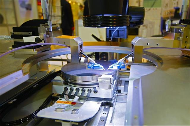
ADLINK has been closely following the evolution of semiconductor manufacturing processes over the years, and has developed a series of probe test solutions that offer the advantages of both high precision and high speed
Photo: Company
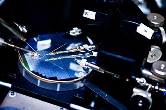
How does the probe station generate a real-time response based on the analog signal generated from contact between the probe and the silicon wafer, thus directing the probe to continue performing the subsequent motion while also ensuring that the probe head accurately and effectively touches the silicon wafer
Photo: Company
DIGITIMES' editorial team was not involved in the creation or production of this content. Companies looking to contribute commercial news or press releases are welcome to contact us.