Leading server chassis manufacturer Chenbro makes a formidable appearance at COMPUTEX 2026 (June 2 to June 5). This year, Chenbro's exhibition flow is strategically designed around three core pillars: Business Development (AI Zone), Product R&D (R&D Zone), and Professional Manufacturing (Manufacturing Zone).The showcase fully highlights Chenbro's comprehensive end-to-end advantages, spanning from precise front-end business alignment and collaborative component design to high-value-added back-end manufacturing services. Furthermore, to address the massive demand fueled by the explosive growth of AI servers, Chenbro is unveiling its newly integrated "Rack Level Solution" for the very first time. Through live physical demonstrations on-site, Chenbro powerfully declares its determination and fruitful milestone achievements as it comprehensively advances into the mechanical components market.Blockbuster Debut: From Server Chassis to Rack Mechanical Integration, Expanding the Innovative Value of AI InfrastructureDriven by the rapid iteration of AI computing architectures, Chenbro officially ventured into the rack mechanical components business last year. Chenbro's CEO stated that industry trends and customer demands have clearly shifted from the "Server Level" to the "Rack Level." Embracing this trend, Chenbro has progressively expanded from traditional chassis to comprehensive rack-level solutions. The physical rack displayed at the exhibition fully demonstrates Chenbro's profound capabilities in mechanical design and manufacturing. With a deep understanding of thermal management technologies (including advanced liquid cooling solutions) and power configuration planning, Chenbro is able to start from the customers' system architecture requirements, translating complex technical demands into optimized mechanical design solutions. By co-developing rack mechanical integration solutions with clients, Chenbro helps accelerate the implementation and deployment of AI infrastructure. The CEO emphasized that amid this technological evolution, Chenbro is no longer solely focused on cost reduction (Cost down); instead, it aims to create higher value (Value up) through system-level collaborative design, truly realizing its strategic vision of becoming a "comprehensive mechanical solution partner."Closely Tracking AI Trends: Heavyweight Exhibition of Next-Generation NVIDIA MGX SolutionsIn the Off-The-Shelf (OTS) exhibition zone, Chenbro leverages modularity as its design foundation, demonstrating highly flexible configuration capabilities that fully cover four major application domains: AI, Cloud, Storage, and Edge computing. As a collaborator of NVIDIA MGX, Chenbro is publicly premiering its 1U NVIDIA Vera Rubin server chassis solution based on NVIDIA MGX, which supports the next-generation architecture. Simultaneously, it is exhibiting a full series of AI chassis products—including 1U, 2U, 4U, and 6U models—developed based on NVIDIA MGX architecture. This powerfully demonstrates Chenbro's top-tier development prowess in satisfying diverse market and customer application needs.Dual Engines of R&D and Smart Manufacturing: Innovative Collaborative Design and the Factory of the FutureTo highlight its ultimate efficiency from R&D to market realization, Chenbro showcases deep technological moats in both its JDM and OEM exhibition zones.Joint Design Manufacturing (JDM): The company displays high-U-count AI servers co-developed with clients, alongside a 21-inch chassis series compliant with OCP ORV3 specifications. By sharing its proprietary JPDP (Joint Product Design Process) and DFM (Design for Manufacturing) optimization mindsets, combined with tolerance analysis and around-the-clock technical services, Chenbro significantly enhances client collaboration efficiency and product stability.Original Equipment Manufacturing (OEM): This zone centers on "Chenbro's Factory of the Future," comprehensively introducing digital and automation technologies. By integrating big data analysis, AI, IoT, robotic arms, and AMR (Autonomous Mobile Robots), the exhibit perfectly demonstrates consistency in product quality and the maximized efficiency of its global localized production.Joining Forces: Building a Win-Win AI Server EcosystemAt this year's COMPUTEX, numerous leading global technology giants are also showcasing AI servers co-developed with Chenbro, fully validating Chenbro's pivotal position in the industry. CEO Corona Chen further pointed out that Chenbro will continue to deepen its partnerships with global CPU/GPU chip companies —such as NVIDIA, AMD, Intel, and Ampere—as well as its core clients, investing heavily in the R&D and manufacturing of next-generation high-end servers. Chenbro will keep exploring the blueprint driving the future of AI, committing to satisfying the diverse application demands of global data centers, and jointly creating a mutually beneficial and prosperous industry ecosystem.For more information , please visit.
PEGATRON Corporation ("PEGATRON") returns to COMPUTEX 2026 in Taipei for the second consecutive year. As a Tech Maker, the company integrates R&D, design, and manufacturing to help customers turn emerging technologies into production-ready products.AI is expanding beyond model training into enterprise and industrial applications. This shift shows that customers need not only computing performance, but also system integration, deployment flexibility, and long-term reliability. Through its AI Tech Maker strategy, PEGATRON turns compute, connectivity, sensing, and product design into deployable systems. PEGATRON will highlight three product areas in Computex: AI infrastructure for AI factories and high-performance computing; edge and industrial AI for manufacturing and communications; and physical AI platforms spanning robotics, drones, intelligent vehicles, and smart devices.Building AI Infrastructure for AI Factory and High-Performance ComputingLarge-scale AI deployment is driving new requirements for computing performance, networking bandwidth, thermal management, and system integration.At COMPUTEX 2026, PEGATRON presents a next-generation AI infrastructure portfolio that includes NVIDIA Vera Rubin NVL72, NVIDIA HGX Rubin NVL8, NVIDIA RTX PRO Server, and AMD Instinct MI355X and MI350P GPU server platforms. The solutions support enterprises and cloud service providers building next-generation AI Factory and high-performance computing environments.PEGATRON also showcases 400G, 800G, and 1.6T AI infrastructure switches designed for large-scale AI training and inference workloads requiring high-speed, low-latency data transmission. Open data center solutions compliant with Open Compute Project (OCP) standards are presented to improve scalability, deployment flexibility, and energy efficiency.The portfolio further integrates GPU servers, AI networking, liquid cooling, and full-rack system integration. This approach expands PEGATRON's role from hardware manufacturing toward comprehensive AI infrastructure platform deployment, helping customers shorten implementation cycles for generative AI, agentic AI, and enterprise AI applications.Bringing AI from Digital Twins to Edge ConnectivityAt the industrial AI layer, PEGATRON presents its PEGAVERSE portfolio, a smart manufacturing platform built around digital twins and agentic AI. The portfolio includes ARCHITECT for site planning, YODA for engineering knowledge training, and JEDI for intelligent manufacturing processes. These applications translate PEGATRON's manufacturing experience into repeatable and deliverable industrial AI offerings.In communications and edge AI, PEGATRON showcases next-generation 5G equipment, AI-RAN concepts, Wi-Fi 7 modules, and 6G antennas. The company is also integrating radio units (RUs) with NVIDIA DGX Spark, reflecting the growing convergence of AI compute and communications infrastructure.PEGATRON also presents its Scalable Central Computing Rack (SCCR) for smart mobility. As a vehicle central computing platform, SCCR integrates IVI, gateway, and ADAS functions, addressing the industry shift from distributed vehicle electronics toward centralized architectures and extending edge computing into mobility systems.Expanding Physical AI Across Ground and Aerial PlatformsAI is moving from data centers into physical environments, where autonomous systems must combine sensing, compute, and motion control to operate reliably in complex conditions. At COMPUTEX 2026, PEGATRON presents ground robot and aerial drone platforms that bring physical AI into mobility systems.SIMBA II, PEGATRON's next-generation quadruped robot platform, combines power electronics, mechanical design, sensing systems, and edge AI computing for inspection, monitoring, and automation tasks. Developed with Swiss precision drive specialist maxon, the platform integrates the HEJ 90 high-performance joint system to improve motion control and stability, while supporting real-time environment recognition and autonomous navigation.The G720 SOM+EVK and AI Companion Computer extend PEGATRON's edge computing and visual perception technologies to intelligent drone platforms. Built on MediaTek's MT8391 platform, they support ROS2 and MAVLink integration with flight control systems and mission workflows, enabling navigation, sensing, and real-time image processing. Vision perception and multi-camera imaging modules further support obstacle avoidance and environmental interpretation.Through its ground and aerial platforms, PEGATRON brings AI compute, sensing, and autonomous control into physical mobility systems, turning related technologies into deployable products.Bringing AI and Design into Smart Endpoint DevicesIn smart devices and user experience, PEGATRON applies its DMS model to combine industrial design, engineering, materials, and manufacturing into the product development process. The M16P Optimus modular laptop uses a modular architecture for key components such as the motherboard, I/O, keyboard, battery, and storage. The design allows flexible configuration based on customer requirements and supports easier maintenance, faster customization, and future platform upgrades.The award-winning Armo Emotion Sensing Game Handle brings sensing technology into interactive applications. It integrates heart rate, electrodermal activity, and temperature sensing to analyze physiological signals and adapt gameplay based on user conditions.In personal care, the PRIIo product line extends PEGATRON's design capabilities into everyday consumer applications. The products combine electronic control, sensing technology, and industrial design for facial and scalp care scenarios.PEGATRON said AI development is shifting from technology-led progress toward practical use. The key is turning innovation into products and systems that can operate reliably over time. The company will continue strengthening its productization and integration capabilities while working with global partners to support technology adoption across different environments.PEGATRON's COMPUTEX 2026 booth is located at L0104, 4F, Taipei Nangang Exhibition Center, Hall 1. Professional guided tours will be available during the show.
Edimax Group will host Expo 2026 during Computex 2026, bringing together its group companies, including EDIMAX Technology Co., Ltd. (TWSE: 3047, including its Edimax and Acelink business units), Comtrend Corporation (TWSE: 8089), and SMAX Technology Co., Ltd. The exhibition will take place from June 1 to June 11, 2026, at Edimax Group headquarters in Taipei.Edimax Group to Showcase AI Edge Innovation at Expo 2026. Credit: EdimaxThis year's Expo carries special meaning as Edimax Group marks its 40th anniversary. Since its founding, the Group has grown from a networking equipment developer into a global provider of connectivity technologies across home networking, enterprise and industrial networking, broadband communications, and AIoT applications.For four decades, Edimax Group has focused on one mission: making technology more reliable, practical, and closely connected to real-world business and lifestyle needs. As the company enters this important milestone year, Edimax Group extends its sincere appreciation to its global partners, customers, and supply chain partners for their long-standing trust and support.Expo 2026 Event InformationEdimax is pleased to announce its upcoming exclusive showcase, centered around the theme "AI Edge. Autonomous Future. Resilient Living." Running from June 1 to June 11, 2026, the event will take place at the Edimax Group Headquarters, located at No. 278, Xinhu 1st Road, Neihu District, Taipei, Taiwan.The showcase will be open from Monday to Friday, 9:00 AM to 6:00 PM. Please note that attendance is by appointment only. We cordially invite industry leaders and partners to schedule a visit and explore the next generation of technological innovation with us.Exhibition FocusExpo 2026 will highlight four key areas: Autonomous Future - AI Edge, autonomous operations, and self-service applications for scalable business growth. Ultra-Speed & Trusted Network - Wi-Fi 8, 25G networking, AI management, and green computing for next-generation connectivity. Secure and Resilient Connectivity - Edge networking and AI-driven management to strengthen security and network resilience. Market-Ready Solutions - Proven, ready-to-deploy solutions that help customers accelerate project launches and market adoption.Edimax Group stated that it will continue to deepen the integration of AI, broadband communications, and smart networking technologies while working closely with global partners to advance next-generation intelligent networks and digital applications.Expo 2026 will be held by appointment only. Global partners and customers are invited to visit and experience Edimax Group's latest innovations, celebrate the company's 40-year milestone, and explore the future of smart connectivity.
JMicron Technology Corp., a global leader in high-speed Bridge IC solutions, today announced it will unveil its flagship innovations at COMPUTEX 2026. Building on years of proven expertise in high-speed interface technologies and strong market recognition, JMicron will present a portfolio centered on extreme performance, intelligent backup, and hyperscale expansion, demonstrating its continued momentum in advancing the digital storage ecosystem.In response to the stringent demands for performance and data protection in big data and professional storage markets, JMicron introduces three key controllers: JMS591, JMS591U, and JMB595.JMS591 is purpose-built for multi-bay HDD array applications, supporting USB 20G and eSATA interfaces. In RAID 0 mode, it delivers read/write performance exceeding 2000 MB/s, providing a powerful foundation for NAS and DAS systems.JMS591U targets enterprise and professional users, integrating JMicron's exclusive Offline Clone & Erase technology. It enables 1-to-4 high-speed duplication and DoD-compliant data sanitization, offering a one-touch solution for data migration and security compliance.JMB595 is a high-performance PCIe Gen4 x4 to 16-port SATA III expansion controller. Through cascading architecture, it can scale to connect up to 240 storage devices, ideally suited for hyperscale data centers and surveillance storage infrastructures."JMicron has long been committed to transforming complex high-speed transmission technologies into intuitive and powerful hardware solutions," said Ming-Cheng Lin, VP of Sales and Marketing at JMicron."The products showcased at COMPUTEX not only push storage performance beyond the 2000 MB/s milestone, but also precisely address customers' critical needs in large-capacity storage and security compliance through integrated RAID engines and offline cloning technologies. We are not merely a chip supplier—we are a strategic partner helping customers build a solid foundation in the data-driven era."JMicron cordially invites global partners and media representatives to visit its booth at COMPUTEX 2026. Through face-to-face engagement and forward-looking technology demonstrations, JMicron looks forward to exploring the future of storage innovation together and ushering in a new era of high-efficiency data transmission and intelligent data management.
At COMPUTEX 2026, Fibocom outlined its perspective on the deployment path of edge AI: as AI moves from the cloud to end devices, the key to large-scale adoption lies not only in model performance, but also in the synergy between stable connectivity and local computing power.Based on this insight, Fibocom continues to strengthen its "Connectivity + AI" capability. On one hand, with wireless modules at its core, Fibocom has built a connectivity product portfolio covering FWA, AI CPE, and next-generation Wi-Fi 8, providing a high-speed, low-latency, and highly reliable connectivity foundation. On the other hand, by leveraging its full-stack AI solutions, Fibocom enhances on-device AI capabilities, enabling terminals with local perception and processing power to improve the stability and responsiveness of AI applications in complex environments.For intelligent edge scenarios, Fibocom launched the Fibocom ClawBox, a high-efficiency AI computing terminal natively compatible with intelligent agents such as OpenClaw and Hermes Agent. Built on a high-performance heterogeneous computing architecture, the product integrates CPU, GPU, and NPU, delivering up to 18 TOPS @ INT8 hybrid precision computing power. With typical power consumption at around 5W, it enables high-density, multi-task parallel inference. It supports multi-stream video analytics, complex visual structuring, voice, and multimodal model inference, while offering low latency, high reliability, and localized deployment capabilities. Combined with Fibocom's Skill Hub, it is widely applicable in security, transportation, robotics, and other intelligent edge scenarios, supporting the large-scale deployment of smart industry applications.At COMPUTEX 2026, Fibocom will showcase a range of innovations at Booth K1022, including AI companion solutions, robotic lawn mower solutions, mobile robotics solutions, and more, demonstrating how "Connectivity + AI" is creating value in high value scenarios. Industry partners are warmly welcome to visit and connect with us.
MSI, a global leader in high-performance computing and industrial solutions, returns to COMPUTEX 2026 (Booth #J0605a) to unveil its strategic AI roadmap. This year's showcase centers on a seamless continuum from data center scale to autonomous edge execution, featuring liquid-cooled AI platforms and supercomputers built on NVIDIA MGX, NVIDIA DGX Station, and NVIDIA DGX Spark architectures.Cloud Foundation: Liquid-Cooled Infrastructure for Hyperscale AITo meet the demands of modern AI data centers, MSI is introducing high-density platforms that prioritize thermal efficiency and performance: CG681-S6093 6U Liquid-Cooled AI Server (based on NVIDIA MGX): Built on NVIDIA MGX architecture, this server supports dual AMD EPYC processors and up to eight NVIDIA RTX PRO 6000 Blackwell Server Edition Liquid Cooled GPUs. It delivers the compute density required for large-scale AI inference - with support for a wide range of agentic, physical AI, scientific computing, simulation, graphics, and video workloads.High-Speed Connectivity: The platform is equipped with NVIDIA ConnectX-8 SuperNICs, providing up to 8×400Gbps Ethernet connectivity for distributed AI environments. Rack-Scale Scalability: MSI's liquid-cooled rack-scale architecture supports up to four CG681-S6093 GPU systems within a 48RU configuration. Networking is anchored by NVIDIA Spectrum-4 SN5600 Ethernet switches and SN2201 out-of-band switches for high-performance AI cluster connectivity.Deskside Development: The Desktop AI SupercomputerBridging the gap between the data center and the developer's desk, MSI presents high-performance AI computing for local workflows: XpertStation WS300 (NVIDIA DGX Station): Powered by NVIDIA GB300 Grace Blackwell Ultra Desktop Superchip with up to 748GB coherent memory and 7.1TB/s HBM3e bandwidth, supporting Windows-based AI development while enabling high-speed CPU-GPU data sharing for large AI models and data-intensive workflows.Efficient AI Refinement: The WS300 is designed for AI model development, fine-tuning, and inference, utilizing a compact, liquid-cooled design with dual 400GbE networking powered by NVIDIA ConnectX-8 SuperNICs to sustain peak performance. (Recently showcased at GTC Taipei).Edge Execution: EdgeXpert and Autonomous IntelligenceMSI is bringing data center-level performance directly to real-world environments through the debut of its edge supercomputing platform: EdgeXpert AI Supercomputer: Built on the NVIDIA DGX Spark platform, EdgeXpert enables enterprises to deploy smarter, faster, and more scalable AI agents and applications at the edge.OpenClaw/Hermes Agent on MSI EdgeXpert: MSI showcases prominent AI Agent frameworks, providing open-source Agentic AI structures that support sustainable local operations and self-optimization capabilities.EU CRA Compliant Agentic AI with Galene Elettra: Powered by a Multi-Agent System (MAS), this solution enables intelligent decision-making across complex workflows while maintaining compliance with the European Cyber Resilience Act (CRA). Legal AI Suite: A specialized platform for enterprise AI, streamlining legal research, document analysis, and IP governance. Smart Campus Patrol: The Smart Campus Patrol Vehicle demonstrates real-time computer vision for precision inspection and smarter industrial operations. Tarot AI Experience with Reachy Mini: An interactive demonstration of Agentic AI, blending robotics with generative AI to deliver personalized engagement. End-to-End AI in Action Across IndustriesMSI delivers purpose-built Edge AI solutions developed with leading industry partners across diverse vertical markets:Smart Manufacturing & Semiconductor:The Edge AI Box MS-C910E with Memorence AI enables real-time machine vision. Partnering with Qiming Tech, MSI leverages the Edge AI Box MS-C939 to deliver real-time, high-precision automated optical inspection (AOI) to optimize semiconductor production yield.Voice AI & Driver Safety: Powered by Ubestream, the Slim Box MS-C926 provides real-time translation, while the Embedded Box MS-C927 enables instant voice-to-order experiences for retail. For driver safety, the In-vehicle Box MS-C932 runs real-time AI Driver Fatigue Detection to enhance on-road security.Smart Transportation & Precision AgricultureIntegrating edge inference with frontline mobility and field operations, MSI optimizes commercial transit and smart farming workflows:Smart Transportation × AI Vision Solutions:MSI is expanding its smart transportation portfolio with mobility solutions powered by Edge AI and in-vehicle vision. The lineup features fleet management tablets, telematics boxes, smart rearview mirrors, and AI-enabled ADAS and DMS systems for fleet monitoring and video analytics. Utilizing real-time AI processing, MSI helps logistics and fleet operators improve management efficiency and strengthen road safety.Smart Agriculture & Drone Integration: MSI introduces an intelligent agricultural solution that seamlessly integrates autonomous drone technology, Edge AI computing, and ground control systems.Built for harsh environments, this comprehensive platform combines drone ground control stations, rugged tablets, T-Box connectivity modules, and centralized multi-drone management platforms. It is engineered for critical use cases including automated field inspection, precision spraying, crop monitoring, and pest/disease identification. By leveraging real-time video analytics, edge inference, and cloud data synchronization, the solution empowers agricultural operators to boost efficiency, streamline operational workflows, and accelerate the transition to smart farming.Extreme Field Mobility (MS-NE21): The NE21 Rugged Industrial Tablet features an Intel 13th Gen Core i Series (Raptor Lake-U) processor, supporting up to 32GB LPDDR5/LPDDR5X memory and 2TB PCIe SSD. Built to MIL-STD-810G standards with an IP65 rating, it survives 4-foot drops and functions from -10°C to 50°C. It offers a 650-nit sunlight-readable 11.6" display with glove/wet-touch modes and a continuous hot-swappable battery system (64Wh to 98.1Wh).Industrial Panel PCs & Robust Hardware FoundationTo support heavy enterprise workloads, MSI highlights its high-reliability industrial hardware portfolio:Industrial Panel PCs: Features include the MS-1A81 (21.5") for Smart Healthcare clinical workflows; the MS-1A22 (12.1") and MS-1A32 (15") for factory floor monitoring; and the MS-1A91 (10.1") and MS-OP01 (15.6") for secure Smart Locker Systems.Hardware Backbone: For multi-industry infrastructure durability, MSI showcases its robust hardware portfolio featuring the Intel Wildcat Lake, NXP, and NVIDIA Jetson Thor series platforms, alongside industrial 4U rackmount systems.Sustainability & EV Charging InfrastructureBringing intelligent infrastructure to the energy transition, MSI presents its smart EV charging solutions:Eco Series Home EV Charger: Awarded the Taiwan Excellence Award, this residential smart charger delivers up to 22kW three-phase output. Powered by NXP industrial MCUs and AI smart control, it integrates with solar storage. Featuring a UL94-V0 fire-rated enclosure (extinguishing over-heat sources in 10 seconds) and RDC-DD leakage detection for underground parking safety, it holds global safety certifications, RPC certification in Taiwan, and $5M USD product liability insurance.MSI Hyper 80 Dual Fast Charger: Designed for urban commercial hubs, this DC fast charger delivers 80kW power distribution within an industry-leading 30cm ultra-slim chassis to maximize space efficiency.Visit MSI at COMPUTEX 2026, Booth #J0605a, Hall 1 (1F), to experience the future of the cloud-to-edge AI ecosystem.Credit: MSICredit: MSI
The global semiconductor landscape is undergoing a fundamental shift, moving from a focus on raw training power to the practical complexities of large-scale deployment. In an in-depth interview, Wallace Kou, President and CEO of Silicon Motion, detailed how the generative AI has evolved beyond its initial stages. While the market's early gaze was fixed almost exclusively on NVIDIA's GPUs, the High Bandwidth Memory (HBM), and the CoWoS advanced packaging technology, Kou argues that the industry is now entering the "Inference" era that is turning previous under-estimation about storage's importance on their head.The Shift from Training to InferenceThe turning point for this realization occurred during the NVIDIA GTC conference in March 2026. CEO Jensen Huang unveiled the Vera Rubin architecture, a move that signaled a massive spike in demand for NAND flash memory. During the initial AI boom, the industry was preoccupied with training massive models, a process that relies heavily on the lightning-fast throughput of HBM. However, as these models move into the inference phase - where they are actually used by end-users to generate content or solve problems - the access to context, historical data, and massive datasets storage become the primary bottleneck.Kou notes a dramatic shift in market sentiment. Only two years ago, storage was often an afterthought in the AI conversation; today, it is a critical scarcity. "There is currently not a single global cloud service provider or major smartphone manufacturer whose demand for DRAM and NAND is being fully satisfied," Kou observed. This supply-demand gap has triggered a financial windfall for storage module manufacturers and memory giants, with some stock prices skyrocketing up to tenfold as the market reacts to persistent shortages and rising prices.Technical Paradigm Shift: CMX and the Infrastructure of ThoughtAt the heart of this transition is a new architecture introduced by NVIDIA: the CMX Context Memory Storage platform. This architecture is designed specifically to handle the "KV Cache" (Key-Value Cache), which allows AI models to remember the context of a conversation or a complex task during the inference process.The hardware requirements for the CMX architecture are staggering in their scale and technical demands. Each individual Rubin GPU requires 16TB of dedicated storage to function effectively within this framework. At a system-level scale, a single NV72 Vera-Rubin setup can demand more than 1 Petabyte, or 1,000 Terabytes, of total storage capacity. Beyond mere capacity, the CMX architecture facilitates direct GPU access to storage, a feature that bypasses traditional latency bottlenecks and ensures that AI inference remains fluid and responsive.While this creates a massive commercial opportunity for the storage industry, it also places an unprecedented strain on NAND production. Kou emphasizes that this is not just a cloud-based phenomenon. The explosion of Edge AI - AI processed locally on devices - is further complicating the supply chain. For instance, driven by major players like Meta, the market for smart glasses is expected to reach 60 million units this year. These wearable devices require high-performance embedded storage, creating a secondary front in the war for NAND capacity.Silicon Motion's Role: Solving the QoS BottleneckAs the world's leading NAND controller maker, Silicon Motion sits at the intersection of these competing demands. The primary technical challenge in modern AI environments is maintaining Quality of Service (QoS). In a multi-tenant cloud environment, where multiple GPUs are accessing shared storage simultaneously for different inference tasks, data transfer speeds can often fluctuate or drop.To solve this, Silicon Motion has deployed its proprietary PerformaShape technology. This technology ensures that even under heavy, concurrent workloads, the transmission speed remains stable. By stabilizing these data flows, Silicon Motion has positioned itself as an "indispensable stabilizer" in the AI ecosystem.Beyond data path optimization, Silicon Motion is also extending its role into system-level infrastructure by providing enterprise-grade boot drives for leading AI GPU, TPU, and DPU platforms, ensuring system reliability and fast initialization at scale.The Crisis of Imbalance: Kou's "Capacity Persuasion" EffortsDespite the record-breaking revenues, Kou is deeply concerned about the "shadows" lurking behind this prosperity. The current memory market is suffering from a dangerous imbalance. To maximize profits and satisfy the insatiable hunger of AI cloud giants, major manufacturers like Samsung, SK Hynix, and Micron are funneling the majority of their capital expenditure (CAPEX) into HBM and DDR5 production.This strategic pivot has effectively "squeezed" the production capacity available for standard NAND flash. Kou warns that this "AI squeezing effect" could lead to a collapse in traditional sectors. Over the past eight months, Kou has embarked on a global mission, meeting with leaders at Samsung, SK Hynix, Kioxia, SanDisk, YMTC, and Micron. His message is one of "capacity persuasion": he is urging these giants to reserve a portion of their production lines for the automotive, PC, and smartphone industries."If these foundational industries break because they cannot find parts, Edge AI will have no 'soil' to grow in," Kou warned. He believes that a total focus on the high-margin AI server market could eventually backfire, destroying the broader technology ecosystem that supports AI development.A Stabilizing Strategy: From Cloud to EdgeSilicon Motion is positioning itself as the "transition enabler" for an industry in flux amid an expected 2–3 year supply shortage. As NAND manufacturers concentrate their internal resources on AI-driven initiatives, they are increasingly outsourcing non-core and mainstream projects, such as PCIe Gen5 controllers and embedded solutions. In this shift, Silicon Motion has emerged as a preferred partner to fill the resulting gap.At the same time, as rising prices weigh on demand in the PC and smartphone markets, the company is helping customers pivot toward automotive and AIoT applications, including rapidly growing segments such as smart glasses, which are seeing a surge in shipments this year.One of the most critical areas is the automotive sector, where Silicon Motion has spent a decade building a presence. While memory giants might see automotive requirements as "niche" or low volume compared to AI servers, Kou views them as essential to global stability. When major OEMs consider abandoning these specialized demands due to capacity constraints, Silicon Motion steps in to ensure the global automotive supply chain does not grind to a halt."We are not just looking for a surge in revenue; we want to fulfill our responsibility to the industry," Kou said. By providing stable controllers and storage solutions for AIoT and automotive applications, Silicon Motion is effectively repairing the cracks in a fractured global supply chain.Future Outlook: 2027 and BeyondThe current supply-demand imbalance is not a temporary glitch but a structural reality that Kou expects to persist until at least late 2027 or 2028. Several factors make it nearly impossible to add capacity quickly, for example, land acquisition is increasingly difficult. The lead time for building specialized cleanrooms and procuring critical equipment now exceeds one year.Kou predicts that while the DRAM shortage might begin to ease by the end of 2027, the relief for NAND will likely come even later. In this high-pressure environment, Silicon Motion's role as a key stabilizing force becomes increasingly important.Particularly in emerging sectors such as smart IoT and automotive applications, Silicon Motion delivers reliable controller and storage solutions, filling the vacuum left by production shifts at major manufacturers or by projects lacking sufficient engineering support.By helping global clients navigate the complexities of geopolitics and capacity wars, Silicon Motion aims to ensure that the AI revolution leads to a steady, sustainable future rather than a chaotic collapse of the broader tech industry.AI inference boom fuels supply-demand imbalance until 2027-2028, says Wallace Kou. Credit: Silicon Motion
Solid State Storage Technology Corporation (SSSTC), a subsidiary of Kioxia Corporation and a leading global SSD provider, is showcasing its enterprise SSDs designed for immersion cooling and engineered for AI-driven data centers, along with a comprehensive portfolio of industrial and enterprise SSD solutions.As generative AI and high-density computing evolve, thermal management is critical. To address this, SSSTC has optimized its SSDs for immersion cooling environments by enhancing corrosion resistance through specialized materials, component protection, and structural design. The lineup includes the SATA ER3, ER4, and ER5 series, as well as the PCIe U.2 PJ1 and EJ5 series.These SSDs are optimized for immersion cooling environments, where systems are submerged in non-conductive dielectric fluids. By leveraging the high heat capacity and convective properties of liquids, heat can be efficiently dissipated through fluid circulation and heat exchange. This approach reduces reliance on traditional air cooling while improving Power Usage Effectiveness (PUE) and overall system reliability.SSSTC is also highlighting a range of industrial and enterprise SSDs optimized for AI and edge applications. Industrial SSDs support Edge AI and harsh environment deployments, with operating temperatures ranging from -40-degrees Celsius to 85degrees Celsius, along with anti-vibration and shock-resistant designs for outdoor and industrial environments. The pSLC architecture enhances endurance for sustained write-intensive workloads, while a multi-tier PLP (Power Loss Protection) framework - including hardware PLP, firmware PLP, and PLN - provides flexible data protection.Enterprise eTLC SSDs are designed to deliver stable performance for AI workloads, offering endurance options of 1 and 3 DWPD over a five-year period for varying workload intensities. Under sustained workloads, they maintain more than 90% random IOPS consistency, minimizing performance fluctuations. Firmware optimized for high-density computing enables low latency operation, while capacitor-based PLP and immersion cooling support ensure reliable performance in demanding deployment environments.With more than 18 years of in-house firmware development expertise, SSSTC understands diverse storage requirements across industries and provides flexible customization options, including configurable over-provisioning, lifespan and capacity optimization, performance and power tuning, and application-specific firmware development. SSSTC remains committed to helping customers build stable, efficient, and sustainable AI storage infrastructures.Founded in 2008, SSSTC became a subsidiary of Kioxia Corporation in 2020 and delivers high-quality SSDs through in-house firmware and NAND expertise. For more information, visit the SSSTC website.Remark: PCIe is a registered trademark of PCI-SIG.Credit: SSSTC
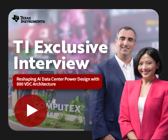
As AI data center rapidly scales toward the gigawatt (GW) level, energy management is evolving from a supporting function into a defining strategic pillar. Against this backdrop, Infineon Technologies is redefining power infrastructure of AI era through its comprehensive "From Grid to Core" strategy, integrating energy efficiency, power density, and system resilience from the electrical grid to the processor core.Scaling AI: Strategic Power Solutions MatterThe evolution of artificial intelligence (AI) has accelerated far beyond the trajectory once predicted by Moore's Law. As AI models continue to expand in parameter scale and real-time inference becomes increasingly critical, demand for computing power is rising at an unprecedented pace.Today, the power consumption of a single GPU is rapidly approaching the kilowatt level, and the power density of a server rack has increased significantly from less than 60kW in the past to exceeding 100kW, now moving toward a new threshold in the megawatt range.This is not just numerical growth; it represents a fundamental shift in power architecture. As AI computing clusters expand rapidly, traditional 48V busbars and AC power distribution architectures are quickly approaching their physical limits in terms of power loss, thermal management, and spatial constraints.Adam White, President of Infineon's Power & Sensor Systems Division, emphasized that future competition in AI infrastructure will no longer be limited to chip performance. Instead, it will be a cross-disciplinary integration battle encompassing power electronics, materials technology, and system architecture.From Grid to Core: Rethinking the power delivery architectureAt this critical turning point for the industry, Infineon's competitive advantage lies not in a single breakthrough product, but in its ability to orchestrate and optimize the entire power delivery chain at the system level."From Grid to Core" is more than a product strategy - it is a multi-phase architectural framework designed to reshape the future AI energy chain. Developed through early collaboration with global hyperscalers and ecosystem partners, the strategy enables Infineon to address evolving AI power demands across every phase of infrastructure, from utility grids to processor-level power management.Power grid: Enabling a sustainable, high-efficiency power with HVDCAt the front end of the data center, power infrastructure is transitioning from traditional mechanical systems to highly integrated solid-state solutions. Future AI facilities are expected to increasingly adopt decentralized DC microgrids, enabling greater efficiency, flexibility, and resilience in energy management.By leveraging silicon carbide (SiC) technology in solid-state transformers (SSTs), system weight can be dramatically reduced - from nearly 20 tons to approximately 500 kilograms—while simultaneously improving overall energy efficiency by more than 1%. Beyond optimizing space utilization and operational costs, this advancement signals a broader industry migration from electromechanical infrastructure toward semiconductor-driven power systems.As SSTs and related technologies become integrated into AI power infrastructure, a multi-billion-dollar semiconductor opportunity is emerging across next-generation energy systems.At the same time, the power grid is evolving beyond its traditional role as just an energy source. Through digitally controlled power systems with real-time monitoring and remote management capabilities, combined with solid-state circuit breakers (SSCBs) featuring microsecond-level response times, the grid is becoming an intelligent energy platform capable of continuous optimization and predictive management.Server rack: Reshaping power density and maximizing efficiencyAs data centers advance toward GW-scale deployments, power distribution architecture is undergoing a fundamental redesign. Infineon is driving the industry's transition from traditional 48V systems to ±400V and 800V high-voltage DC architectures. Through the design of three-phase power sidecars, Infineon is restructuring power supply and computing systems to establish a more efficient and flexible power distribution model.At the same time, the power architecture of AI data centers is following a clear evolutionary path: moving from integrated server rack designs to high-voltage DC and sidecar power supply configurations, and ultimately advancing to gigawatt-scale infrastructures that incorporate DC microgrids.Meanwhile, The high-frequency characteristics of gallium nitride (GaN) components enable intermediate bus converters (IBCs) to achieve over 98% conversion efficiency and exceptionally high power density in an extremely compact form factor, significantly reducing power transmission losses and freeing up more space for AI computing resources.Processor core: Power density and new architectures for next-gen AI computeAt the processor core—the final stage of power delivery—the challenge shifts toward managing extreme current density and ultra-fast transient response.To support next-generation GPUs requiring massive current delivery and rapid load transitions, Infineon has introduced a digital multiphase PWM controller alongside the industry's first TLVR four-phase power module. These technologies are engineered to provide highly stable, efficient, and responsive power delivery for AI processors operating under increasingly demanding workloads.In response to the next generation of GPUs demanding ultra-high current and rapid load changes, Infineon has introduced digital multiphase PWM controllers and the industry's first TLVR quad-phase module. By leveraging high-precision telemetry and digital control technologies, power systems have transformed from energy suppliers into intelligent platforms capable of real-time monitoring, prediction, and optimization.From AI data center to physical AIIf data centers form the foundation of AI computing power, the physical world will be where AI's true value is ultimately realized. As AI increasingly expands into humanoid robots, autonomous systems, and intelligent manufacturing equipment, demands for energy efficiency, real-time responsiveness, and system reliability will become even more critical.Infineon is extending its long-established expertise in power management beyond data centers into the emerging era of Physical AI. By integrating sensing technologies, actuate, security and connectivity solutions, and high-efficiency power modules, the company is enabling a comprehensive functional blocks that empower humanoid robots to perceive, think, act and connect, safely and secured in a real-world environment.Push the boundaries of power technology in AI era"We Power AI" is not just a slogan for Infineon—it is a concrete commitment to the future of the industry. From gigawatt-scale data centers to physical AI, Infineon continues to push the boundaries of power technology, ensuring that every watt of energy is transformed into the greatest possible value for AI.As the industry advances toward the next generation of computing, energy management will become the decisive key to truly unlocking the full potential of AI. In this wave of transformation, Infineon is joining forces with ecosystem partners to stand at the forefront of defining the future.Editor's Note: Adam White will deliver a keynote address at COMPUTEX 2026 on June 4 titled "Infineon Powering AI from Grid to Core to Physical AI." The session will explore emerging trends and strategic opportunities in power infrastructure of AI era.Credit: Infineon
Elitegroup Computer Systems (ECS), a leading global provider of motherboards, mini PCs, and computing solutions, will participate in COMPUTEX 2026 from June 2 to 5, 2026, at Taipei Nangang Exhibition Center, Hall 1, Booth J1317a. Under the theme Power AI Computing, ECS will present its latest motherboards and LIVA Mini PCs, highlighting how compact and scalable PC platforms can support AI Agent workloads, Edge AI processing, smart healthcare applications, and embedded deployments.ECS will demonstrate how LIVA Mini PCs can be flexibly deployed in edge computing environments to support AI-assisted information retrieval, private knowledge base applications, healthcare data monitoring, and embedded commercial deployments. Through these demonstrations, ECS will highlight the role of LIVA Mini PCs in data processing, application execution, real-time monitoring, and vertical use cases. ECS will also showcase motherboard platforms with high-performance expansion capabilities, providing customers with a broader choice of computing foundations for AI and edge applications.Showcasing AI Agent Applications in PC EnvironmentsECS will showcase OpenClaw AI Agent applications running on an AMD desktop PC at its booth, demonstrating how AI Agent capabilities can be applied in PC-based environments. The demonstration will cover common scenarios such as system status queries, information search, and content summarization, showing how AI Agents can help users streamline daily operations and improve information processing efficiency. Through this demonstration, ECS will further present the flexibility and practical value of integrating AI Agent applications into commercial PC environments.LIVA Z11 PLUS. Credit: ECSLIVA One H810. Credit: ECSExtending Edge AI into Healthcare and Private Knowledge ApplicationsECS will showcase the LIVA Z11 PLUS mini PC in two Edge AI and data-driven scenarios: healthcare monitoring and private knowledge base applications. In the healthcare demonstration, the Z11 PLUS will support hemodialysis simulation and FHIR BOX applications, showing how a compact mini PC can serve as an edge computing node for medical data collection, real-time monitoring, and data format conversion.The knowledge base scenario will run a local database with a natural language interface, enabling users to query product and business information more intuitively. This highlights the role of mini PCs in enterprise information access, private data environments, and on-site applications where sensitive information needs to be managed locally. Powered by Intel Core Ultra processors, the LIVA Z11 PLUS provides high-speed storage, dual networking, and USB4 connectivity to support data-intensive Edge AI applications.LIVA Z15 PLUS. Credit: ECSExpanding the LIVA Lineup from AI-ready Performance to Embedded FlexibilityBeyond AI application demonstrations, ECS will present its full LIVA Mini PC lineup and next-generation platforms for commercial, edge, and embedded deployments. The new LIVA Z15 PLUS, built on the Intel Wildcat Lake platform with integrated NPU-based AI acceleration, will be a key highlight of ECS’s LIVA showcase, addressing high-performance commercial use, AI-assisted workloads, and edge computing applications.ECS will also feature the LIVA One H810, extending the LIVA One series' upgradeable socket-type design with the Intel Core Ultra LGA1851 platform. For low-power and embedded applications, the LIVA Z4F offers fanless reliability, while the LIVA Q4 combines an ultra-compact form factor with 45W USB Type-C power input for mobile, space-constrained, and flexible installation environments.