ASMPT will be exhibiting at SEMICON Taiwan from September 10 to 12, 2025. The theme of the presentation at Booth L0716 at Level 4, TaiNEX 1 in Taipei is: "Empower the Intelligence Revolution." This refers to the driving forces for new chip technologies like AI, smart mobility, and hyperconnectivity. As a leading provider of advanced packaging and semiconductor assembly solutions, ASMPT enables its customers to develop cutting-edge AI technologies, supporting both high-performance AI chips that integrate advanced memory technologies like HBM and efficient components for edge devices. ASMPT will showcase three machines at SEMICON Taiwan: the new ALSI LASER Platform, the fine-pitch wire bonding solution AERO PRO, and the SIPLACE CA2 uniting semiconductor and SMT processes.

ASMPT will be exhibiting at SEMICON Taiwan from September 10 to 12, 2025.ASMPT
The next-generation LASER platform has been specifically developed to meet the increasingly complex requirements of IDM and Foundry semiconductor companies for laser dicing and grooving wafer materials. This new system with ASMPT's patented multi-beam technology expands the company's portfolio with a focus on front-end operations.
"The new platform combines high-precision laser processing with smart automation to support the next generation of semiconductor manufacturing", says Patrick Huberts, Head of Business and Marketing at ASMPT ALSI. "It's the ideal platform for applications in advanced packaging, AI, and power automotive. We invite you to join us for the official launch and discover the new machine live at our booth during SEMICON Taiwan."
High-performance wire bonding
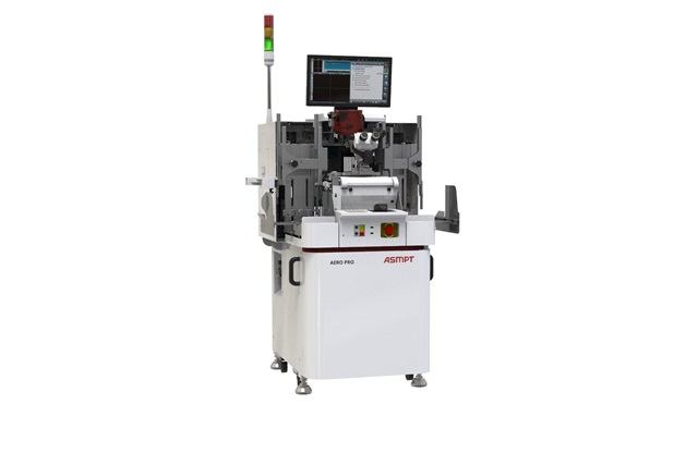
ASMPT also introduces its latest high-performance wire bonder at SEMICON: the AERO PRO. Developed for high-density semiconductor designs, this machine delivers the highest bonding accuracy and exceptional speed for wires with diameters of 0.5 mil (≈12.7 µm). Thanks to integrated real-time monitoring and preventive maintenance functions, the system is ideally suited for use in intelligent, networked production environments. To accommodate complex designs such as system-in-package (SiP) and multi-chip modules (MCMs), as well as applications like ball grid arrays (BGAs), land grid arrays (LGAs), memory modules, or quad flat packages (QFPs) with external leads. For uniform 22-µm bond balls, it employs the patented X-POWER 2.0 transducer—a lightweight and vibration-optimized ultrasonic transducer that supports mixed-wire and vertical bonding in bond via array (BVA) technology. Optimized for complex interconnects in memory, microcontroller units (MCUs), and more, ideal for advanced applications such as AI edge devices and automotive systems.
Bridging Semiconductor and SMT
The hybrid SIPLACE CA2 placement solution from ASMPT SMT Solutions redefines advanced packaging by uniting semiconductor and SMT processes in a single, high-speed platform. Traditionally, die bonding and SMT placement were separate steps — now, they are seamlessly integrated. Designed for advanced packaging applications in smartphones, 5G, AI, high-performance computing (HPC), and IoT devices, the SIPLACE CA2 processes both SMDs from tape and dies taken directly from sawn wafers. This eliminates the need for expensive die taping, saving up to 800 km of tape annually in 24/7 production, reducing both cost and material waste. With up to 76,000 components per hour (cph) for SMT, 54,000 cph for Die Attach, and accuracy of up to 10nm @ 3σ accuracy, the SIPLACE CA2 delivers high-speed and accuracy — even for advanced Die Attach and Flip Chip applications. A breakthrough buffer system decouples die pickup from placement, solving previous speed limitations. Up to 50 wafers can be managed with just 13 seconds of swap time – unmatched in the industry.

The SIPLACE CA2 boosts productivity in advanced packaging by combining classic surface-mount technology with die-attach and flip-chip assembly. ASMPT
Article edited by Jack Wu