

iCometrue received enthusiastic responses following its show at SEMICON TAIWAN 2023. Some companies have expressed great interest in iCometrue's Logic Drive and Field Programmable Multi-Chip Package (FPMCP) and approached iCometrue for further discussion.
iCometrue is making every effort to bring Logic Drive to reality. As the costly non-recurring engineering (NRE) and time-consuming process put up a high barrier preventing IC designers' access to sub-10-nm fabrication technologies, iCometrue proposed the concept of Logic Drive in 2016, to create a Public Innovation Platform that enables 99% of the common public to participate in cutting-edge technology available to the wealthy 1%.
Field Programmable Gate Array (FPGA) chips manufactured on sub-10-nm nodes are suitable for realizing Logic Drive. With 10 nm and more advanced processes, tens of billions of transistors and more than 15 metal layers can be placed on a silicon chip, and the power supply voltage can be scaled down to 0.7V. By packaging one or more standard commodity FPGA chiplets using advanced packaging technology, such as TSMC's CoWoS or InFO or Intel's EMIB, and pairing it with a non-volatile memory (NVM) chip (for example, a flash memory chip) to store the FPGA configuration data, the Logic Drive is made into a non-volatile field-programmable standard commodity, which can be mass commercialized as an ASIC chip after configuration.
Whether iCometrue's Logic Drive will become a reality hinges on FPGA standardization. If FPGA becomes a standard commodity like DRAM, the cost will significantly decline. For FPGA standardization, iCometrue proposes retaining the programmable circuits of the FPGA while removing the I/O circuits and control circuits to form new chips, namely, an I/O chip and a control chip, which are also packaged in the same Logic Drive. This way, most of the area of the FPGA chip is used for the arrays of logic cells (logic block array), similar to the layout of DRAM cell arrays (memory block array). Standard specifications should be established for the FPGA chip size, the circuits, and quantity of logic cells, as well as the I/O layout, quantity, electrical properties, and functions (including driving capability and impedance as well as inter-chip communication). iCometrue chairman Dr. M. S. Lin urges that it's time to standardize FPGA!
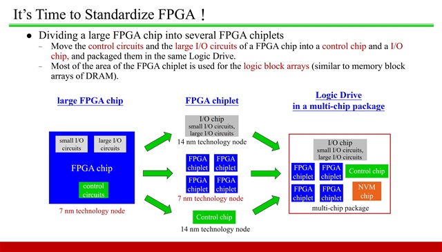
With FPGA standardization, most of the area of the FPGA chip is used for the arrays of logic cells (logic block array), similar to the layout of DRAM cell arrays (memory block array).
Photo: iCometrue
iCometrue is also cooperating with partners to develop FPMCP, wherein an FPGA chip and NVM chip are added to a multi-chip package (MCP) comprising CPU, GPU, ASIC, and/or SOC. Through configuring or re-configuring the FPGA chip, the MCP becomes field-programmable, and with the NVM chip to store the FPGA configuration data, the FPMCP becomes non-volatile and field-programmable.
iCometrue is working on an FPGA/NVM package unit that packages an FPGA chip together with an NVM chip for use in a customer's MCP. It is also seeking partners interested in applying the FPGA/NVM package unit to practical applications.
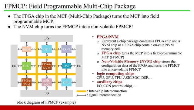
Through configuring or re-configuring the FPGA chip, the MCP becomes an FPMCP and with the NVM chip to store the FPGA configuration data, the FPMCP becomes non-volatile field-programmable.
Photo: iCometrue
Last but not least, also in the spotlight at SEMICON TAIWAN was Dr. Lin's book, Moore's Journey –The Magical Power of Big Numbers. Giving an in-depth look into the past and present of semiconductors and Moore's Law, the much-raved-about book has inspired and benefited a great many readers.

