
CONNECT WITH US
Sign out

TSMC fab construction in Japan mainly requested by its largest client, says CEO CC Wei

, Taipei
0

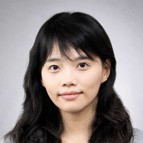
TSMC CEO CC Wei; credit: DIGITIMES

TSMC's decision to build a fab in Japan, though not a low-cost place, was made mainly at the request of its largest client, as prioritizing customer needs has been always the foundry's core consideration, according to company CEO CC Wei.

Wei made the remarks when asked what motivated TSMC to set up a fab equipped with 22/28nm processes in Japan, at a recent forum on "The New Challenges in the Semiconductor Industry" hosted by Mount Jade Global Science and Technology Association in Taipei.

He said TSMC has a customer in Japan that happens to be a major supplier of its largest client, and the company must give its full support to the Japanese customer to ensure that the production schedule of its largest client will not be affected, otherwise its 3nm/5nm fabs could see orders impacted.

Industry sources said Apple is TSMC's largest client, contributing about 25% of its annual revenues, while Japan's Sony is an important supplier of image sensors for iPhones. The foundry is building a new 12-inch fab in Japan's Kumamoto in cooperation with Sony and Denso, which is set to start commercial production of 22/28nm chips by the end of 2024 at a monthly capacity of 55,000 wafers, with 12/16 nm process technology also to be incorporated.

Wei also noted the biggest problem for building a fab in Japan is the lack of talent. To solve the problem, he added, more than 200 Japanese engineers are being trained at TSMC's Taichung fab, and the foundry will also send 500-600 engineers to serve at the joint-venture fab.

When asked by an audience member to comment on Japan's latest move to form a semiconductor alliance with the US to develop 2nm process technology, Wei pointed out that while it's not impossible for a business or a country to take shortcuts in semiconductor manufacturing, it would be difficult.

He continued that before developing 2nm process node, Japan does not have any technology development roadmaps for 3nm, 5nm, 7nm and even 10nm processes. Japan in fact seeks to leapfrog, which would usually end with "getting your insurance company to pay."

Wei also pointed out that TSMC's investments are mainly made to support its development roadmaps for at least two and a half years ahead. In other words, its 2022 capital expenses are aimed at development needs for 2025 and beyond.

TSMC's cooperation with customers has also been kick-started well ahead of commercial production. For instance, Wei said, if a client's chip products are now being fabricated at TSMC with 3nm process technology, related cooperative preparations should start three years ago.

Article translated by Willis Ke