German startup NanoWired GmbH has been announced as one of the winners in the Taiwan Innotech Exhibition (TIE) 2022 innovation award competition. TIE will be hosted from October 13 to 15 at the Taipei World Trade Center Exhibition Hall 1, and a virtual exhibition hall is available for visitors who cannot attend in person. DIGITIMES Asia talked to Olav Birlem, CEO and co-founder of NanoWired, at its Taipei Tech Center.
Q: Could you give a short introduction to the origin of the company and the background of the founders? How big is the team?
A: NanoWired GmbH is a spin-off from the Technical University of Darmstadt. The foundation of NanoWiring technology was laid there. By combining the technical know-how of three members of the institute and the market knowledge and industry experience as well as investor money of me, we decided together to industrialize the NanoWiring technology and to go the way of changing electronics and electrical engineering in the field of interconnection technology. Thus, an initial juice press technology became an industrial NanoWiring technology. It enables different joining techniques such as KlettWelding (joining at room temperature), KlettSintering (copper sintering at 170°C) and KlettGluing (the ideal anisotope gluein). NanoWiring is done today on a 300x400mm format. We provide PCB, FPC, LTCC, leadframes and wafers up to 300mm on any substrate with NanoWiring structures. From four employees in the beginning, a team of 25 employees has grown up in Germany. In addition, we have three employees in the TechCenter Taiwan, which will also be expanded to 20 employees in the coming years.
Q: Can you explain your technology? What inspired you to develop this technology? What challenges have you overcome? Has this NanoWiring been adopted by semiconductor companies in Europe?
A: The NanoWiring process works a bit like a pad printing process. We have a sponge that carries the electrolyte. It has a special porosity layer on the bottom. We then use a stamp to press the sponge against the substrate, let some current flow through it, and thus deposit metal. This can be copper, for example, but gold, silver and nickel are also possible. After electroplating the NanoWiring structures, the sponge is removed. A stripping process is used to remove all other materials that are unnecessary for the further process. The substrates thus provided with NanoWiring structures, for example IGBT, µC, D-RAM, sensors, foils, glasses, ceramics or circuit boards, are simply placed on top of each other and cold pressed together. The ideal electrical, thermal and mechanical contact is ready. We realize contacts in the range between 3um and 300mm. If the NanoWiring structures are only applied to one substrate, a low-temperature KlettSintering process is available.
With our technology with the nanowires, we have the opportunity to compensate for a higher unevenness of surface and even a higher level of particles that you can't see, but for semiconductors are critical. So, with our technology, you can make the additional joining under ISO 6 and I say even ISO 8 level with micro pads the size of three micrometers, so that this non-wiring structure, you have the opportunity to compensate these planes with this.
For example, if you make hybrid bonding, we make hybrid material bonding. So, that hybrid is the same, but we have the hybrid in the material and the others have the hybrid in the bonding principle. This request of ISO 2 level reduces the number of players who are able to handle this technology even from the cost perspective with our technology.
We also solve the energy loss problems, because our contact is resistance free. So, if you make a journey with us, there is no measurable resistance inside anymore. The electronic losses inside, especially for frequency converters, battery packing, and battery management, is reduced tremendously by our copper joining technology.
The inspiration to develop the many different interconnection technologies is the solution of the problems from the intensive customer discussions and customer projects but also the solution of the problems I experienced in my own more than 25 years of professional practice.
NanoWired cooperated with some European car OEMs, tier-1 suppliers, and chip IDMs from the first minute of its foundation. Even though this intensive customer contact may have made development more restless, the direct industry connection paid off. The biggest challenge was to earn the respect for the NanoWiring technology and the NanoWired team in the industry. This in spite of all the failures to keep inspiring people to trust and in the end raise money that NanoWired would move forward with its technology. The other main challenge was to develop from a university team into a professional team that works with our customers on an equal footing.
On the other hand, we collaborate in many funded public projects as a central novel packaging technology and enabler for the next step in performance or development. Actually, there is no semiconductor manufacturer in Europe that does not collaborate with us. We have applications in power semiconductors from SI, SiC to GaN, 2D and 3D integration with chiplet technologies and stacking of dies, as well as the use of our ISO KlettWelding-Tape technology for fan-out substitution with bond wires. Our collaboration also extends far west and does not stop at large water masses. Since we also work closely with upstream processes and downstream processes in Europe, a perspective series of production with existing equipment is easily possible. The process that needs to be retrofitted is only NanoWiring and stripping. The rest is there.
Q: You have set up an R&D center in Taipei. What prompted you to set up this facility in Taiwan? How many employees do you plan to hire in Taiwan for your projects?
A: For me, Taiwan is the center of uC (microcontroller) production. Nowhere in the world are so many companies, technologies, processes and knowledge compactly together as in Taiwan. On the other hand, Taiwan is very centrally located to reach other Asian electronic centers like Japan, Korea or Thailand. So I made the strategic decision to make the routes to Taiwan, the center of uC manufacturing. So our NanoWired TechCenter connects NanoWiring technology with your industry. We are currently starting with three employees who are also flanked by personnel from our HQ and will expand to 30 employees with our customers and investors.
Q: Are you planning to raise funds this year or next year? What is the current status of funding? Since we learned that JX Nippon is your newest investor, are there any other large companies investing in NanoWired?
A: Taiwan knows how intensive investment in the development of semiconductor technologies is. NanoWired has very strong investors such as JX-Nippon, Walden International, and WIKA. NanoWired will be doing another Series B fundraising early next year. We are focusing on additional European as well as international investors. The goal is to raise capital for the next growth step, not only to further industrialize the NanoWiring machine but also to raise the processes and structures to an international level. In general, however, the investors in NanoWired do not only provide money. Another important aspect is to accelerate the maturity of the company and to enable additional networks for growth.
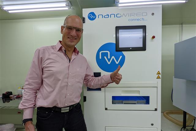
NanoWired CEO Olave Birlem in front of a machine that cultivates nanowires
Photo: DIGITIMES Asia, October 2022