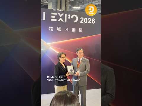
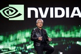
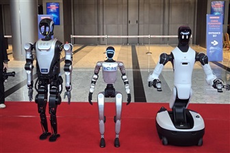
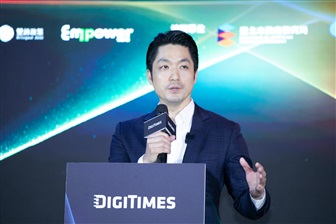
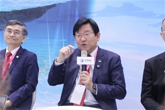
Driven by a wave of massive technological investments and strategic corporate partnerships, Taipei City is rapidly transforming into a premier global hub for Artificial Intelligence. Speaking at the highly anticipated AI Expo Taiwan 2026, Taipei Mayor Wan-an Chiang outlined a comprehensive vision for the city's economic and structural future, highlighted by landmark commitments from industry titans such as Nvidia, Google, and key domestic supply chain players like Wistron.
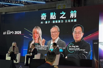
Quantum computing is shifting from isolated experiments toward hybrid architectures integrated with high-performance computing and artificial intelligence (AI), speakers said on March 25 at the AI Expo Taiwan 2026, as the industry looks to position quantum systems as components within data center infrastructure rather than standalone research platforms.
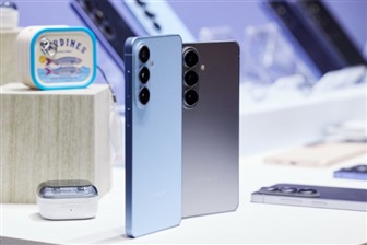
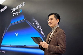
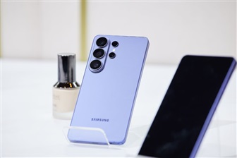
Samsung Electronics officially announced a transformative update to its Quick Share solution, marking a historic shift in the mobile industry by introducing native compatibility with Apple's AirDrop protocol. Beginning March 23, 2026, the South Korean tech giant is rolling out this cross-platform functionality, starting with the newly released Galaxy S26 series. This move represents the first time a Samsung smartphone has natively bridged the gap to Apple's notoriously closed sharing ecosystem, effectively ending years of digital isolation between Android and iOS users.