CONNECT WITH US
Thursday 20 August 2026
Chroma's Proprietary ASIC Technology Reshapes the Semiconductor Test Landscape
As demand for AI servers, high performance computing (HPC), and data center infrastructure accelerates, the semiconductor and power electronics test equipment market is experiencing strong growth. This momentum is expected to continue as advanced semiconductor technologies drive increasingly sophisticated testing requirements
Thursday 20 August 2026
Chroma's Proprietary ASIC Technology Reshapes the Semiconductor Test Landscape
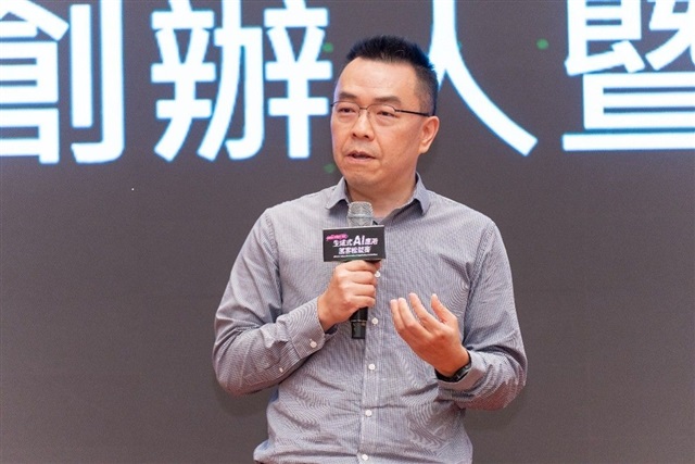
As demand for AI servers, high performance computing (HPC), and data center infrastructure accelerates, the semiconductor and power electronics test equipment market is experiencing strong growth. This momentum is expected to continue as advanced semiconductor technologies drive increasingly sophisticated testing requirements.Chroma ATE Inc., a company with more than two decades of experience in automated test equipment (ATE), recently held its Semiconductor Test Equipment User Conference in Hsinchu, Taiwan. Registration quickly reached capacity, reflecting the company's growing prominence in the semiconductor testing market. In 2025, Chroma reported consolidated revenue of US$943 million and grew its global workforce to nearly 4,000 employees.Credit: ChromaGeorge Chang, President of Chroma's Semiconductor Test Equipment Business Unit (STE BU), emphasized that Chroma is one of the few ATE suppliers with the in-house capability to develop  application-specific integrated circuits (ASICs) for its own test systems. This capability creates a "technology moat" that reinforces Chroma's competitive advantage.To address the diverse needs of the semiconductor testing market, Chroma has built its portfolio around three specialized test platforms. The Chroma 3680 is designed for advanced devices used in AI, HPC, microcontroller unit (MCU), and mixed-signal applications, the Chroma 3650 addresses power devices and systems-on-chip (SoCs), and the Chroma 3380 targets mainstream MCUs, Internet of Things (IoT) devices, and other chips manufactured on mature process nodes. Combined shipments across the three platforms have exceeded 4,000 systems. This year, Chroma also introduced the compact Chroma 3650-S2C platform for high-power devices, responding to increasingly rapid product cycles across the semiconductor industry.Credit: ChromaProprietary PINF ASIC Enables Seamless Migration for Complex SoC TestingAs AI and HPC drive more complicated chip designs, testing is becoming more diverse and technically more demanding. At the same time, the industry is facing growing pressure to reduce costs and shorter test development schedules. Spancer Lee, Senior Manager of product marketing at Chroma's STE BU, explained that the Chroma 3680 integrates Chroma's next-generation, self-developed PINF ASIC with a range of specialized system boards, each supporting different test functions. This architecture enables comprehensive coverage across four major testing domains: digital, analog, mixed-signal, and RF devices. Chroma plans to continue expanding the platform's capabilities, leveraging the flexibility of its in-house hardware development to support high-precision testing of increasingly complex and high-frequency SoC devices. To accommodate the intensive data transfer and processing requirements involved with testing advanced semiconductor devices, the Chroma 3680 employs an 8-lane, 20 Gbps parallel high-speed data architecture. Optimized firmware enables high-speed transfer and more efficient processing of complex test data. The architecture also minimizes synchronization latency between digital and analog resources, improving resource integration for highly complex SoC test programs.The Chroma 3680 architecture is also compatible with certain probe card models used on competitor platforms. This allows customers to retain existing load boards and test programs without modifying their hardware, reducing migration costs while maximizing ROI and helping chipmakers gain a competitive edge in the market.Credit: ChromaChroma 3650-S2C Delivers High-Voltage Capability in a Compact FootprintWith NVIDIA signaling a transition toward direct 800V DC power delivery for server racks, semiconductor manufacturers face growing demand for high-voltage testing. To address this need, Chroma developed the 3650-S2C, a new test platform optimized for high-power semiconductor devices including silicon carbide (SiC) and gallium nitride (GaN). Through extensive engineering refinement, the platform's slot count was reduced to six, optimized for the requirements of intermediate-level testing. Chroma also substantially streamlined the external high-voltage power rack by integrating it directly into the test head. The 3650-S2C cuts the system footprint by half, enabling seamless integration with mainstream turret handlers for volume production while helping OSAT partners save valuable factory space and infrastructure costs.Aaron Chuang, Senior Manager of Advanced Technology Development at Chroma's STE BU, highlighted two key characteristics of the Chroma 3650-S2C: powerful high-voltage capability and a compact footprint. Building on the proven Chroma 3650-S2 platform, the solution integrates a high-voltage source-measurement unit (HVSMU) board to deliver a comprehensive, one-stop solution for five critical test parameters. It enables customers to safely and accurately overcome the 4 kV test threshold while maintaining production throughput, providing a powerful foundation for next-generation high-voltage power semiconductors to advance into mass production.Credit: Chroma???????Integrated High-Density RF Technology Addresses Next-Generation Ultra-High-Frequency Wireless TestingThe rapid adoption of AI, edge computing, and intelligent connected devices continues to drive growth across Wi-Fi, Bluetooth, GNSS, IoT, mobile, and wearable applications. At the same time, wireless communication chipsets are undergoing a significant generational upgrade.To address these evolving requirements, Chroma has integrated its new HDRF3 (high-density radio frequency) test module into the Chroma 3680 platform. The solution is designed to support the increasing bandwidth, advanced modulation schemes, and multi-antenna architectures required by next-generation wireless technologies. This positions the company to capture the high-performance networking and AIoT chip packaging and testing markets.According to Jackson Hsu, associate director of application engineering at ADIVIC, a Chroma-affiliated company, Wi-Fi 7 expands channel bandwidth from 160 MHz to 320 MHz while increasing modulation density to 4096-QAM. These advances place exacting demands on RF performance and noise characteristics in test instrumentation. The HDRF3 test module was specifically developed to meet these requirements, extending operating frequencies up to 8 GHz and providing full coverage for Wi-Fi 7 as well as future Wi-Fi 8 implementations.ADIVIC also plans to launch an extension model, the 35809, featuring a simplified 16-port design while maintaining complete software compatibility with the production-oriented HDRF3 platform. The solution is targeted at applications requiring RF IC testing only. Chroma's in-house ASIC expertise allows the company to adapt the hardware architecture of its Chroma 3680, 3650, and 3380 platforms to distinct market requirements. From the space-efficient Chroma 3650-S2C to the high-density HDRF3 module, each development addresses emerging technical challenges across the semiconductor industry.Credit: ChromaThrough a combination of flexibility, high return on investment, and seamless platform migration strategies, Chroma helps customers accelerate adoption while reducing operational barriers. As AI, advanced computing, wireless connectivity, and power semiconductors continue to reshape the industry, Chroma is positioning itself as a long-term strategic partner for the world's leading semiconductor manufacturers.
Thursday 20 August 2026
Henkel Launches LOCTITE ABLESTIK CDF900 Series Conductive Die Attach Film
Henkel Adhesive Technologies today announced the launch of Loctite ABLESTIK CDF900, its next-generation conductive die attach film (cDAF) series, at SEMICON Taiwan 2026. Delivering thermal conductivity exceeding 8 W/m-K, the new material is designed to help semiconductor manufacturers overcome rising thermal and stress challenges in AI, 5G and emerging 6G telecommunications, and high-performance computing (HPC) applications.As AI, HPC, and next-generation communications drive higher chip frequencies, greater thermal design power, and more complex package architectures, efficient heat dissipation and stress control have become critical to device performance and reliability. Loctite ABLESTIK CDF900 addresses these challenges by combining high thermal conductivity with the precision and process consistency of a film-based die attach format.Technical Breakthrough for High-Performance AI Packaging"Henkel is a global leader in conductive die attach film, with technology widely adopted in Wi-Fi communications, automotive electronics, and power devices. Today, Loctite ABLESTIK CDF900 pushes thermal performance to new heights while expanding applications into large-die packaging scenarios such as processors and AI chips. This offers customers broader design flexibility and superior thermal management solutions," said Kaihua Zhou, Head of Market Strategy for Semiconductor at Henkel Adhesive Technologies Electronics.The core breakthrough of Loctite ABLESTIK CDF900 lies in its proprietary thermal filler technology, which substantially increases thermal conductivity to more than 8 W/m-K. This enables high-power components in mobile phones, processors, and Wi-Fi equipment to dissipate heat efficiently and maintain stable performance in demanding operating environments.Compared with competing liquid die attach adhesives, Loctite ABLESTIK CDF900's film-based format helps eliminate the risks of material bleed-out and non-uniform bondline thickness. This enables chip designers to achieve smaller, more precise die footprints within constrained spaces while enhancing overall package reliability and robustness.Complete Material Solutions to Address Stress Challenges in AI Advanced PackagingTo address warpage during processing and component stress issues inherent in large-die advanced packaging, Henkel continues to expand its material portfolio. The company has developed high-thermal-conductivity liquid molding compounds, high-performance capillary underfills, and diverse packaging material platforms to meet requirements for efficient heat dissipation, high reliability, and process flexibility. By reinforcing structural strength, toughness, and adhesion, Henkel's materials help mitigate stress imbalances while meeting the stringent reliability and high-volume manufacturing stability requirements of high-end AI packaging.At SEMICON Taiwan 2026, Henkel will present its complete portfolio for critical advanced packaging applications, including underfill, conductive die attach film, liquid molded underfill, and non-conductive liquid adhesive technologies.Kevin Becker, Senior Vice President of Product Development and Engineering, added, "These solutions support board-level to wafer-level packaging, low to high thermal conductivity applications, and small to large die footprints. Leveraging its comprehensive product portfolio, global R&D resources, and localized technical support, Henkel empowers customers to improve thermal performance, package reliability, and mass-production readiness in advanced package designs, while providing vital material support for the next generation of AI development."Global Footprint and Multi-Site Support Deliver Supply Chain ResilienceAmid geopolitical shifts and global expansion, semiconductor supply chain resilience has become a priority in international procurement decisions. Henkel has established a robust multi-site support network and operates manufacturing facilities across North America, Europe, and Asia, with established production and technical support hubs in Taiwan, South Korea, China, Japan, and Southeast Asia. Flexible backup production sites enable localized, real-time support to meet global customers’ capacity expansion and procurement flexibility needs.Sustainability Commitment: Advancing Circularity in Semiconductor MaterialsSustainability is a core value at Henkel. In material R&D, the company has pioneered the integration of eco-friendly product design methodologies. For example, Henkel is collaborating with partners to advance circular economy practices, including the use of silver powder from recycled silver, a precious metal widely used in semiconductor packaging. Henkel is committed to working hand in hand with industry partners to reduce carbon emissions and minimize resource waste.Visit Henkel at SEMICON Taiwan 2026During SEMICON Taiwan in September, Henkel will present its full suite of material solutions for advanced packaging and high-performance semiconductor applications in Room 404, Hall 1 of the Taipei Nangang Exhibition Center. The company will showcase its technical capabilities across AI infrastructure, HPC, next-generation communications, and Edge AI.The hospitality suite will feature a variety of interactive experiences, creating opportunities for customers and industry partners to engage directly with Henkel's technical experts. Together, participants will explore innovative solutions for advanced packaging, including thermal management, reliability enhancement, stress mitigation, and readiness for high-volume manufacturing. Through collaboration and knowledge exchange, Henkel continues to support the semiconductor industry's progress toward higher performance, greater reliability, and enhanced resilience.Details about Henkel consumer electronics materials are available here, and information about its semiconductor solutions can be found here.LOCTITE is a registered trademark of Henkel and/or its affiliates in the USA, Germany and elsewhere.
Wednesday 19 August 2026
SK hynix Accelerates 40 Trillion won Share Repurchase and Cancellation
SK hynix Inc. (or "the company", www.skhynix.com) announced today that its Board of Directors has approved a resolution to repurchase and fully cancel 40 trillion won worth of its own shares. The Company also revealed plans to return "over 50% of cumulative Free Cash Flow (FCF)" generated during the program period (2025-2027), adopting a framework centered on the parallel execution of share repurchases and cancellations alongside cash dividends.Following the Board meeting held earlier today, the Company formally disclosed the share repurchase and cancellation resolution along with the shareholder return plan via a regulatory filing.The decision stems from the assessment that the Company's intrinsic value—underpinned by its business competitiveness, robust cash generation capability, and mid-to-long-term growth potential—is not fully reflected in its current stock price.SK hynix continues to record record-breaking financial performance, maintaining its leadership in the AI memory market. As of the end of the second quarter of this year, the Company's net cash stood at approximately 69 trillion won, demonstrating significantly improved cash generation capability.The total planned amount for the share repurchase is 40 trillion won. Based on the closing stock price of 1,662,000 won on the day prior to the Board resolution, this represents approximately 24.07 million shares, or about 3.3% of total issued shares (730,492,365 shares). The repurchase period is scheduled to run for approximately three months starting August 20, with all repurchased shares set to be cancelled upon completion of the acquisition.This initiative accelerates the execution of the existing shareholder return program ahead of schedule. In November 2024, SK hynix announced a program to execute shareholder returns within the range of 50% of its three-year (2025-2027) cumulative FCF, noting that it would consider early execution prior to the program's expiration if FCF increased meaningfully due to improved operational performance.The 40 trillion won program marks the largest treasury share cancellation ever conducted by a South Korean listed company. The Company noted that progress toward its financial health targets remains on track, affirming its commitment to maintaining a stable financial structure while delivering sustained shareholder value.Through today's regulatory filing, SK hynix announced plans to pursue an expansion of its total shareholder return target from the previous "within 50% of cumulative FCF" to "over 50% of cumulative FCF". Under the framework, shareholder returns will be executed through a dual-track approach running share repurchases/cancellations alongside cash dividends, while options to expand payouts—including the existing fixed dividends and special dividends—are also under consideration.SK hynix emphasized that it intends to pursue additional shareholder returns within the program period through the parallel execution of share repurchases/cancellations and dividends, by taking into account cash flows, market conditions, and distributable profits, adding that specific details regarding scale and execution will be announced following Board approval at the time of its third-quarter earnings release.