
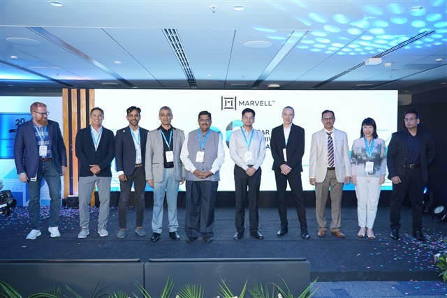
Marvell Technology has opened 100,000 square feet of additional semiconductor R&D space in Bengaluru and plans to double its India headcount over the next three years as part of a US$250 million investment program.
Navin Bishnoi, Marvell's vice president and India country manager, told DIGITIMES that the company is also constructing another 140,000 square feet at its Bengaluru campus and 125,000 square feet in Hyderabad.
The new Bengaluru wing became operational several weeks before its formal opening on July 29.
Marvell said the three-year investment would expand its technology capabilities, workforce and engineering infrastructure. Bishnoi said the spending would include R&D, product development, capital expenditure and operating costs.
The company entered India in 2006 with fewer than 50 engineers. It now employs more than 2,000 people directly across Bengaluru, Hyderabad and Pune, making India its second-largest R&D organization globally. Marvell plans to double that workforce over the next three years, although it has not disclosed a precise hiring target.
From execution to product ownership
Bishnoi said India had historically been viewed largely as an execution center, with local engineers implementing specifications developed elsewhere. That model has changed as the company has added senior technical roles and given India-based teams greater responsibility for chip architecture and product delivery.
"We have moved from execution to architecture ownership and product ownership," Bishnoi said. Indian teams hold product responsibility in areas including security, networking, wireless and carrier infrastructure.
Bishnoi cited the company's data-center security products as one area where development leadership is based in India. Local teams handle architecture and product delivery, while foundry engagement, manufacturing, packaging and supply-chain work remain distributed across Marvell's global operations.
Product-roadmap decisions generally stay close to the company's largest customers, many of which are based outside India. India-based architects nevertheless work directly with customers during implementation, including on custom-silicon programs.
Role grows in custom silicon and advanced nodes
Marvell is expanding its custom-silicon business as hyperscalers seek processors designed for specific AI workloads and data-center architectures.
Indian teams develop subsystems used in those chips, including memory interfaces, input-output blocks, security functions and on-chip interconnects. These components can be combined into designs tailored to individual customers.
Bishnoi said Indian engineers were involved in custom-silicon programs for hyperscalers and large enterprise customers, but no single India-based team was responsible for an entire custom XPU.
Developing such a processor can require hundreds of engineers working across IP design, EDA, testing, manufacturing and advanced packaging, making it a global undertaking. Indian engineers are also participating in Marvell's advanced process-technology work.
The company said its teams in India have expertise in 2-nanometre and more advanced technologies, high-speed analog IP, subsystem development, software and firmware, and end-to-end silicon development.
Marvell is also using AI tools across RTL design, verification, design-for-test, physical design, firmware and silicon validation. Bishnoi said verification had shown the clearest productivity gains, followed by physical design and software development.
Advanced packaging limits local manufacturing engagement
India's growing role in Marvell's design operations has not yet translated into local packaging and testing work. Marvell is speaking with Indian outsourced semiconductor assembly and test companies, but their current capabilities do not meet the advanced packaging requirements of its leading AI products.
Many Indian OSAT projects are initially focused on established packaging technologies. Marvell's AI products require chiplet integration and advanced packaging capabilities such as 2.5D and 3D integration, Bishnoi said, adding that no Indian OSAT provider currently had the required capability or planned to offer it in the short term.
The company will continue to assess local providers as their technology plans develop, but Bishnoi said commercial engagement remained some distance away.
He expects the next phase of the India Semiconductor Mission to place greater emphasis on advanced packaging. Building the required ecosystem will take sustained investment and time, he added.
"This is a patience game," Bishnoi said, adding that developing the ecosystem would be a decade-long journey.
Article edited by Jerry Chen