Advanced Chip and Circuit Materials today announces the commercial availability of Celeritas HM50 and Celeritas HM001, which eliminate the root causes of warpage, package bow, solder fatigue, and high-frequency signal loss in large-format AI accelerators and advanced chip packaging architectures. Celeritas HM50 is a negative CTE (-8 PPM/°C) material and Celeritas HM001 is a near-zero CTE material. Used together in a single stackup, they bring board CTE below 10 ppm/°C while simultaneously delivering Tier 9 electrical performance.
Every hyperscaler building AI infrastructure is confronting the same pair of converging constraints. As AI accelerators scale beyond reticle limits, thermomechanical mismatch between silicon (2–4 ppm/°C) and standard PCB materials (~18 ppm/°C) produces catastrophic reflow warpage, package bow, and solder joint fatigue. Simultaneously, the explosive growth in data rates, driven by HBM, UCIe, and chip-to-chip interconnect operating at 100+ Gbps, is pushing signal integrity requirements beyond what standard PCB dielectrics can support. The industry has been searching for two separate solutions to two separate problems. ACCM has built one material family that addresses both.
The industry's leading proposed fix of solid glass substrates remains positive in CTE and does not address the electrical side at all. ACCM today announced Celeritas HM50 and Celeritas HM001, which together solve both problems simultaneously. Programs can start today.
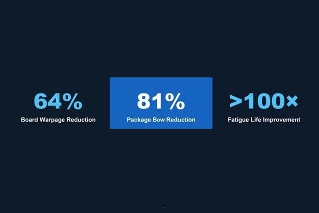
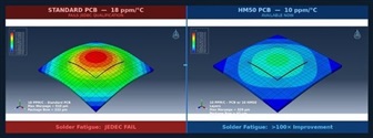
Celeritas HM50 FEA – Standard PCB at 18 ppm/°C (left) vs. PCB with HM50 at 10 ppm/°C (right). FR4 PCB baseline fails JEDEC qualification, while the PCB with HM50 shows >100× improvement. Warpage and Package Bow are reduced by 64%, and 81%, respectively. Combined HM50+HM001 stackups achieve even lower effective CTE.
Keshav Amla, COO of Advanced Chip & Circuit Materials, said,"Rather than incrementally tuning stackups, we are applying a breakthrough materials innovation to remove a fundamental limitation that has constrained system scaling. HM50, with its negative CTE of -8 PPM/°C, drives the effective CTE of the board down. Even with heavy copper designs, you could tune a board down to 12, 10, 8 PPM/°C or lower. And where next-generation data rates demand extreme loss performance, HM001 replaces those layers with a Tier 9 loss material that has a near-zero CTE. Together, they give designers headroom they simply have not had before."
The HM Class of materials matches each layer type in an AI accelerator stackup with a material purpose-built for it: HM50 for the power planes, HM001 for the signal layers.
As AI accelerators grow in scale, the industry has long struggled with two separate problems — boards warping under thermal stress, and signal loss at extreme data rates. ACCM's Celeritas material family tackles both within a single solution. Celeritas HM50 counteracts the thermal expansion mismatch that causes warpage and solder joint failures, enabling designs that previously failed industry qualification to now meet it with significant margin. Celeritas HM001 addresses the signal integrity side, supporting the data rate demands of next-generation AI interconnects while also contributing to thermal stability. Together, the two materials give chip and board designers headroom that standard PCB materials have not been able to provide. For more details, please visit here.
Credit: Advanced Chip and Circuit Materials