
Created less than four years ago as a joint venture between the Germany-based Infineon Technologies and Taiwan-based Nanya Technology, Inotera Memories is now seen as an example of the achievements of Taiwan's semiconductor industry. Earlier this year, Inotera completed its initial public offering (IPO), listing on the Taiwan Stock Exchange (TSE) in March. The company currently operates one 300mm plant in Linkou, Taoyuan County, with a monthly capacity of 65,000 wafer starts, and production will be fully converted to a 90nm trench process by the end of the third quarter. In November, Inotera will begin moving in equipment at its second 300mm facility in Linkou, deploying 90nm trench technology from the initial stage of the plant's operation. According to the company, the total capacity of its two Linkou plants will reach 95,000 wafer starts per month by the middle of 2007.
Prior to this year's SEMICON Taiwan, DigiTimes.com had an opportunity to sit down with Inotera president Charles Kau, who is also the chairman of the SEMICON Taiwan 2006 IC Committee, to discuss the event, company developments and the current status of Taiwan's DRAM industry.
Q: As the chairman of the SEMICON Taiwan 2006 IC Committee, what would you say the show means for Taiwan's DRAM industry and Taiwan's IC industry?
A: You know that SEMI Taiwan opened its office in Hsinchu in the beginning of 1996, but I started working together with the organization, supporting their conferences and other activities, since the early 1990s. Its main and most important contribution to Taiwan's IC industry, as I think, is that SEMI consolidates all the forces within the industry. It is more than a community. SEMI provides a platform for all of us, including semiconductor manufacturers, equipment makers and material suppliers, to be gathered in one place, discussing problems and finding solutions.
SEMICON Taiwan is naturally a big part of the efforts that consolidate the industry and facilitate its development. On the one hand, engineers get a good opportunity to know more about manufacturing processes and learn modern trends in materials and equipment by visiting the showcase. Apart from an educational purpose, SEMICON Taiwan serves as a place for company executives to talk about the industry in its current stage and outline further developments by participating in forums and conferences.
Q: One of the topics scheduled to be discussed at this year's SEMICON Taiwan is the future transition to 450mm (18-inch) wafer production, though the industry has not yet completed the transition to 300mm (12-inch) wafers. What do you think, looking ahead?
A: It is an interesting topic for discussions, and although I will hopefully retire to playing golf and fishing before the real transition begins, scaling up to 450mm wafers, as a task, will gradually increase its significance. I have no doubts in that.
So far, I only see a contradiction, which is not yet answered within the industry. The contradiction is between big players of the semiconductor industry, on the one hand, and suppliers of materials and equipment, on the other hand. While pushing a faster scaling up schedule, big players, such as Intel, may face opposition from suppliers, which seem not that interested in moving ahead too fast. Big players aim to increase revenues and profits by transitioning to larger wafers. For smaller companies, it will be a question of survival, since many of them will hardly be able to afford the cost of transition. This means that suppliers of materials and equipment may lose their customers.
The semiconductor industry scales up wafer sizes every 12 to 15 years in average. In the past, such transitions were always accompanied by a decreased number of companies that could afford the manufacturing costs at the new level. For example, while over 100 companies worldwide produced 200mm wafers, only about 50, perhaps even less, were able to move ahead to production on 300mm wafers. Approximating a similar trend going to the next phase, which will be the transition to 450mm wafers, it is easy to understand why suppliers are already worried about the future.
By the way, to a much lesser extent, similar concerns were also expressed regarding scaling down to smaller process nodes.
Q: Some industry experts and analysts expressed concern that trench DRAM designs may not be able to advance beyond 65nm. Do you consider this a challenge?
A: I would say that both stack and trench designs have their own challenges in scaling down to 65nm and beyond. For the stack design, the main issue is how to maintain required levels of storage node capacitance with taller stacks, and it should be addressed by further improvements in chemical vapor deposition (CVD) machines. The trench design, on the other hand, will have to manage making deeper and narrower trenches, but so far, I do not see any physical barriers or limitations that would make moving beyond 65nm impossible. Together with our technology partners, we are already working on a 58nm process.
From a business viewpoint, there is concern of another sort. There are currently five major groups in the DRAM industry, and four of them develop stack technology. And because stack technology accounts for about 75% of the global market, equipment suppliers seem more interested in targeting this market segment. Some people in the industry consider this a potential threat to the only trench design group - which is led by Qimonda, and includes Nanya as a technology partner and Inotera as a production base for these two companies - saying this camp will face more problems with equipment supply in the future.
Q: Do you ignore these sort of claims?
A: There is no way to ignore them, but you should not forget that our group, which holds about 25% of the global market, currently represents a bigger market share than any of the remaining four stack design groups, counted individually. Moreover, the four major stack designs are not compatible with each other. If some equipment is not sold to one group, suppliers cannot simply offer it to any other group. Of course, if trench technology loses its positions to the competition, equipment suppliers will lose an interest to work with us. But it will only happen if we are not successful in our own market.
Q: What do you think about the consolidation processes in the DRAM industry? Do you expect any merges or acquisitions in the foreseeable future?
A: In my opinion, the industry infrastructure is complete, so I do not expect more merges in the near future. There are five groups - which I previously mentioned. Within these groups, I think, relationships will become closer, including mutual investments.
Q: There is an opinion that in the future, consolidation may involve pure-play foundries, such as Taiwan Semiconductor Manufacturing Company (TSMC) or United Microelectronics Corporation (UMC). What do you think about this?
A: Watching it becomes more interesting, especially since UMC started increasing its stake in ProMOS this summer. That is all that I can say at the moment.
Q: While Taiwan is known as a key region in the global IT industry - and its industries dominate in various market segments - many Taiwan-based IT companies continue expanding their production facilities in China. However, players in the semiconductor industry, including DRAM makers, face legal restrictions from Taiwan's government. Do the restrictions really hinder development in the DRAM industry?
A: While amounting to nearly 1.5% of total operating expenses, labor costs are not that critical for the semiconductor industry. I think that saving labor costs should not be the main reason to expand to China.
By maintaining the cheapest cost for wafer production, Taiwan currently has the world's best infrastructure for semiconductor manufacturing, which is very efficient. In Taiwan, if a machine fails, you do not even need to change into your street clothes. Here, with all key material and equipment suppliers concentrated in close proximity, you typically get a problem of this sort solved in 20 minutes. In most other places, including China, you do not need to be in a rush to report the problem - have a cup of coffee or cigarette first - as there is not much chance for the problem to be quickly fixed.
If a company such as TSMC, for example, sees China as a key potential market, it may make more sense to establish production facilities there. If saving labor costs is the only driving force, the expansion strategy will not be that effective.
Q: Founded in 2003, Inotera is the youngest DRAM producer in Taiwan. How does the company plan to develop its business? Can you tell us about Inotera's roadmap for expansion? Does the company consider NAND, NOR or any other type of flash memory a potential area for business development?
A: Inotera was established as a foundry that exclusively provides manufacturing services to Infineon (now Qimonda) and Nanya, and at this point, we do not plan to change this business model. The important thing to understand is that our company is not a DRAM company, and in the future, we will not become a DRAM company.
As a manufacturing service provider, Inotera is not focused on shipping commodities to the market. Instead, we fill internal manufacturing needs of commodity suppliers. Yes, we currently have 100% of our capacity reserved for DRAM wafer production, but later, after two years or longer, the situation may change. We are not in a rush to take the decision.
Inotera will continue serving two customers for DRAM manufacturing, but we are still considering sensors and NAND flash as potential areas of diversification, and we may decide to work with more clients in these new areas. Since we can leverage relationships with existing customers as a way to lower diversification risks, I think that entering NAND production should be easier for Inotera. NOR is another story. As long as it does not become a commodity, we will not manufacture this type of flash memory.
Q: How big is Inotera's R&D budget? Do you plan to increase it in the future?
A: With R&D primarily focused on yield improvements, the R&D budget currently does not exceed 1.5% of our revenues. Moving to smaller process nodes, we will likely increase it.
Q: Do you think that Taiwan companies should play a more active role in the development of memory standards? Does Inotera plan to become a member of JEDEC or the Memory Implementers Forum (MIF)?
A: At the moment, not. So far, we are not ready for a lot of laboratory work that a JEDEC membership implies. I think that two years from now, Inotera will join JEDEC, and I agree that Taiwan's DRAM industry should be more active in standard developments, synchronizing its efforts with overseas companies. In fact, I already see Taiwan DRAM companies deepening their R&D collaboration with technology partners abroad, and in the future, development will definitely be more synchronized.
Q: What do you think about the prospects for Taiwan's DRAM industry, as a whole, in the near-term and long-term? Do you see a chance for Taiwan to lead the global DRAM industry, much as Taiwan dominates in other IT segments?
A: Since over 30% of the global DRAM manufacturing is concentrated in Taiwan, I see a big chance for Taiwan's DRAM industry to become the global leader. Leveraging its strength in manufacturing, the industry is actually able to repeat the success of Taiwan foundries. I would not be surprised, if after five years, Taiwan produce 45% of all DRAM in the world.
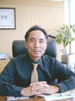
Charles Kau: "SEMI provides a platform for all of us, including semiconductor manufacturers, equipment makers and material suppliers, to be gathered in one place, discussing problems and finding solutions."
Photo: Vyacheslav Sobolev, DigiTimes.com
Article edited by Vyacheslav Sobolev