

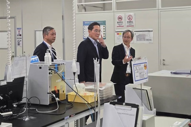
Samsung Electronics chairman Lee Jae-yong visited the company's Advanced Package Lab (APL) in Yokohama, Japan, on November 1, as the chipmaker looks to Japan's semiconductor materials and equipment industry to strengthen its advanced packaging capabilities...
The article requires paid subscription.
Subscribe Now