
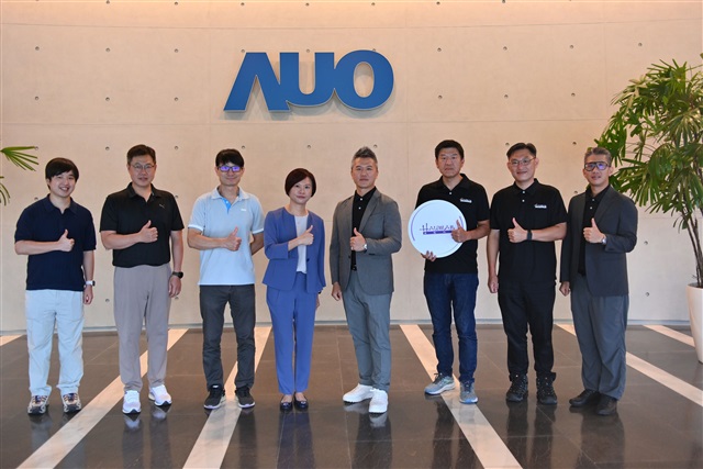
As AI-driven high-performance computing (HPC) and chip-to-chip optical interconnects continue to see rapid growth, Hauman Technologies, a leader in test and measurement solutions, has introduced a breakthrough GHz-class, massively parallel bandwidth testing technology in collaboration with AUO Corporation. Designed to address testing efficiency and throughput bottlenecks for next-generation optical communication light sources, the technology made its official debut at SEMICON Taiwan on September 2.
Overcoming Mass-Production Bottlenecks with Parallel High-Speed Testing
For years, high-frequency characterization of Micro LED chips has relied on time-consuming, die-by-die measurement procedures. While these methods are well suited to detailed device characterization, their limited throughput presents a major challenge for industrial-scale production and broader commercial adoption.
Hauman's newly unveiled Micro LED response-time measurement technology addresses this challenge by enabling simultaneous, parallel high-speed testing across multiple dies. With temporal resolution down to 20 picoseconds (ps), the technology captures the transient optical response of individual light sources at different time intervals, enabling key bandwidth-related parameters to be derived without conventional dynamic scanning.
By shifting high-speed characterization from sequential measurement toward parallel acquisition, Hauman aims to bring die-level high-speed screening closer to the throughput requirements of semiconductor manufacturing.
Advancing Optical Interconnect Testing in Collaboration with AUO
The collaboration combines Hauman's 20-picosecond temporal resolution and high-throughput parallel measurement capabilities with AUO's expertise in optoelectronic integration, Micro LED mass transfer, and low-power optical engines.
Together, the companies are working to optimize Known Good Die (KGD) screening for optical communication devices, supporting next-generation AI data centers and "wide-and-slow" optical interconnect architectures.
"Our latest technology represents a major step forward in high-frequency testing throughput and the viability of production-scale deployment," said Ying-Chu Lin, Vice President of Hauman's Semiconductor Business Division. By enabling parallel measurement across multiple dies while maintaining die-level visibility, we aim to bring high-speed optical characterization closer to the requirements of semiconductor manufacturing.
We look forward to working with semiconductor, optoelectronic device, and packaging and testing industry partners to further advance high-throughput optical measurement for next-generation optical interconnects. For more information, please visit Hauman Technologies.

Credit: Hauman Technologies