
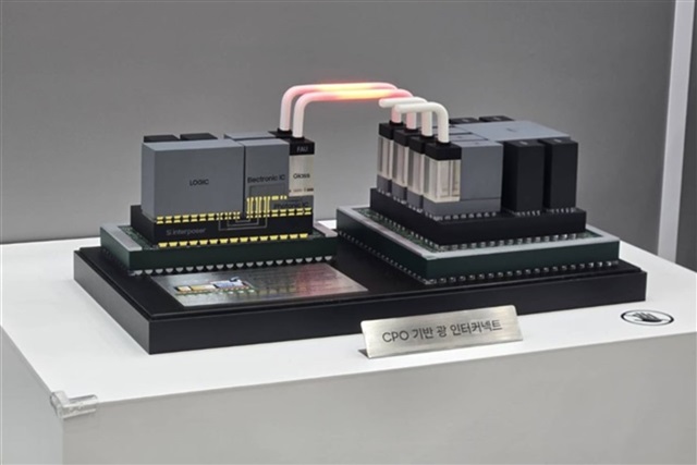
Samsung Electronics' packaging technology lead, Lee Hee-seok, outlined the company's advanced semiconductor packaging roadmap at Advanced Semiconductor Packaging & Chiplet Show (ASPS) 2026...
The article requires paid subscription.
Subscribe Now