


CONNECT WITH US
Sign out

ASE launches first automated PLP line, eyes 1H27 production

, Taipei
0

Credit: DIGITIMES

Advanced Semiconductor Engineering (ASE) has unveiled its industry-first automated panel-level packaging (PLP) system, a development poised to reshape global artificial intelligence (AI) and high-performance computing supply chains by significantly improving chip integration speeds and manufacturing efficiency for AI data centers and cloud infrastructure providers.

Panel production takes shape

Mass production is scheduled to begin in the first half of 2027, following the planned opening of the manufacturing line at the company's Kaohsiung facility by the end of 2026. Upstream equipment suppliers from various regions have already delivered initial machinery since the second quarter.

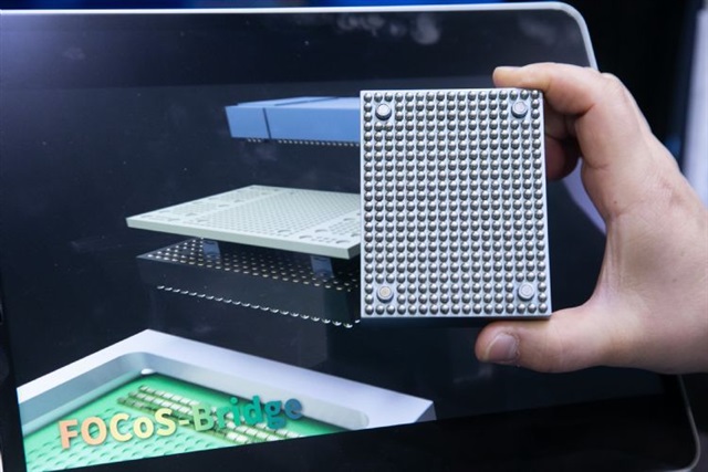
The new system supports the 310×310mm format and works with advanced packaging platforms, including FOCoS and FOCoS-Bridge. It delivers precise 2×2μm and 8×8μm spacing capabilities. Company executives describe the deployment as a critical step in moving from traditional wafer-level manufacturing to larger panel-based processes.

Why panels beat wafers

EVP Yin Chang noted that expanding AI workloads demand faster, more efficient connections between chiplets, application-specific integrated circuits, and high-bandwidth memory. Industry analysts agree that switching to rectangular panels solves longstanding manufacturing bottlenecks.

By replacing circular wafers with larger sheets, manufacturers can increase usable surface area by approximately 96,100 square millimeters per panel. This expansion allows more chips to be packaged simultaneously, reduces material waste, and accelerates production cycles. The shift is particularly vital for AI data centers and supercomputing applications that require larger package sizes and higher connection density.

The road to heterogeneous integration

The panel-based approach is viewed as a foundational architecture for complex multi-trillion-transistor designs. Automated manufacturing lines are essential for achieving the economies of scale required to commercialize these systems. By minimizing tool changes and streamlining large-area processing, the platform aims to address persistent challenges in performance, power consumption, and manufacturing scalability.

The technology is expected to support a broad range of sectors, including AI computing, high-end gaming, and edge computing devices, marking a decisive transition toward heterogeneous integration across the global semiconductor industry.

Article translated by Jingyue Hsiao and edited by Jerry Chen
