CONNECT WITH US
Sign out

South Korea eyes memory-led AI order against Nvidia

Daniel Chiang, Seoul
0

Credit: DIGITIMES

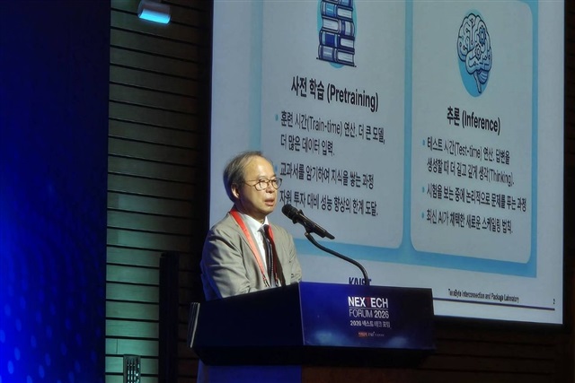
As AI shifts from training to inference and from single-task use to multi-agent collaboration, South Korea's semiconductor industry is seeking to recast the market around memory rather than GPUs. South Korean academia and industry figures say the AI era will be defined by memory architectures, with the country aiming to build its own framework and challenge an order long dominated by Nvidia.

Korea Advanced Institute of Science and Technology (KAIST) professor Kim Joung-ho said at a forum that memory and storage used to be subordinate to CPUs, but South Korea should now create a memory-centered hierarchical architecture. From SRAM to memory fabs, he said, memory should sit at the center, with CPUs and GPUs becoming subordinate to memory instead.

He said AI models work by absorbing and calculating vast amounts of data, and the more input data they receive, the more accurate the output becomes. That shifts the bottleneck away from raw computing power and toward data-transfer speed, helping drive the rise of high bandwidth memory (HBM).

HBM stacks memory chips vertically, expanding data pathways from the dozens to the thousands and lifting bandwidth by orders of magnitude. At the same event, SK Hynix advanced memory solutions head Shim Jun-seop said that in Nvidia's flagship GPUs, for example, the H100 and H200 have nearly unchanged compute-core specifications, but HBM capacity rises to 141GB and bandwidth increases by about 40%, ultimately boosting inference performance by 42%.

The limits of GPUs

Inference has recently replaced pre-training as the main battleground for AI, and differences in model architecture are no longer the main decisive factor. Instead, "how much context data can be called during inference" has become the key measure of AI capability, raising the importance of memory further.

Kim said Claude's alleged leaking of internal source code suggests that the memory required for real-world multi-agent operation could be more than eight times higher than estimated. Multiple agents running in parallel, evaluating one another, and keeping background sessions active all consume massive memory resources.

That is putting Nvidia's business model under structural pressure, he said, because GPU stacking has physical limits that further elevate memory's importance. Heat dissipation makes it difficult to keep scaling centralized GPU computing, while communication latency between GPUs means that simply adding more GPUs can actually reduce efficiency.

A new memory architecture

Facing rising dependence on South Korean memory makers, Nvidia is also moving to build its own memory and storage ecosystem. It plans to use data processing units (DPUs) together with an inference context memory storage (ICMS) architecture to create an independent data-scheduling network based on NAND Flash, reducing its reliance on SK Hynix and Samsung Electronics and helping boost NAND makers such as SanDisk.

Despite that, Kim argued that routing data through external network paths still carries inherent disadvantages in latency and efficiency. He said that South Korean industry should seize the opportunity to establish its own network architecture for memory, linking HBM, high-bandwidth flash (HBF), and memory modules directly through high-speed interfaces such as PCIe Gen 7 so that most AI inference computing can be completed at the memory layer, leaving CPUs and GPUs in a supporting role.

According to current test data, the proposed architecture raised throughput by nearly 100 times when running inference on a 405-billion-parameter large model, and this is now being actively promoted toward major companies. But under that scenario, overheating in GPUs and memory becomes even more severe, and cooling is expected to be the factor separating winners from losers in the semiconductor industry over the next 10 years.

At present, mainstream HBM uses a 2.5D packaging architecture. Although memory is stacked vertically, it still connects to GPU processors through a silicon interposer in a planar layout.

South Korean industry is now pushing toward true 3D integration, directly stacking processors and memory vertically in hopes of proactively defining system architecture and driving a new semiconductor revolution.

Article translated by Lily Hess and edited by Jack Wu