
CONNECT WITH US
Sign out

SK Hynix accelerates advanced packaging from Korea to Indiana

, Lillian Chen, DIGITIMES Asia
0

Credit: AFP

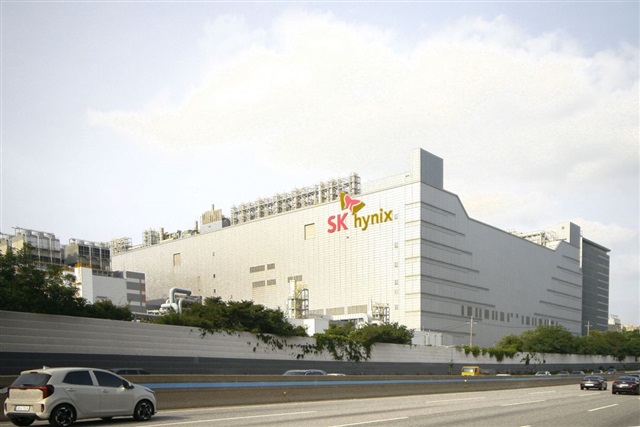
SK Hynix plans to invest KRW19 trillion, about US$12.9 billion, to build an advanced semiconductor packaging plant in Cheongju, South Korea, as it moves to secure capacity for AI-driven memory demand. The investment would add to existing packaging operations in Icheon and a planned facility in Indiana, creating a network spanning South Korea and the US.

South Korean media reported that the Cheongju facility, designated P&T7, is scheduled to break ground in April 2026 and is expected to be completed by the end of 2027. SK Hynix said the project is intended to meet rising demand for high-bandwidth memory, or HBM, as competition intensifies in AI-focused memory.

Industry sources said packaging capacity has become a key constraint as large technology companies increase spending on AI infrastructure. SK Hynix is expanding capacity as rivals Samsung Electronics and Micron step up efforts to ramp AI memory products.

Indiana project and the case for speed

SK Hynix currently conducts most of its AI memory packaging at its P&T4 facility in Icheon. In April 2024, it announced plans to invest US$3.87 billion to build an advanced packaging and R&D facility in West Lafayette, Indiana, but opposition from some residents has complicated the process.

Against that backdrop, SK Hynix selected the Cheongju Technopolis industrial park for P&T7 after considering links to front-end manufacturing, logistics, and operational stability. The site offers closer integration with existing production and clearer execution timing for the investment.

Technology and market position

Packaging capability remains central to SK Hynix's effort to defend its lead in HBM. A key technology is its proprietary Mass Reflow Molded Underfill, or MR-MUF, process used in stacking memory chips for high-performance applications.

Market participants expect that further packaging advances could support broader offerings, including a one-stop supply of HBM alongside packaging services. AI accelerator 2.5D packaging is largely dominated by TSMC, and expansion into that area could further differentiate SK Hynix.

According to Reuters, SK Hynix led the global HBM market last year with a 61% share, followed by Samsung Electronics at 19% and Micron at 20%, based on data from Macquarie Equity Research. SK Hynix is also Nvidia's main HBM supplier, underscoring the strategic importance of expanding packaging capacity.

Article edited by Jack Wu
