
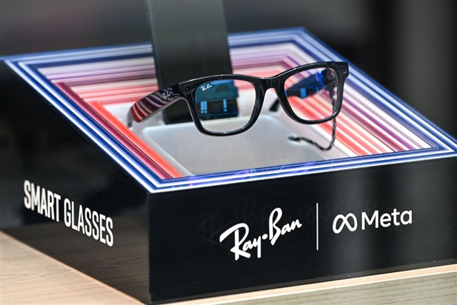
As the global semiconductor industry eyes the rise of 12-inch silicon carbide (SiC) wafers as potential game-changers in advanced packaging, a surprising development is reshaping the conversation. A Chinese startup has reportedly discovered a high-value application for large-diameter SiC substrates—one that directly aligns with the supply chain of tech giant Meta's AI-powered smart glasses.
This breakthrough, industry insiders say, signals not only a potential inflection point for China's compound semiconductor industry but also opens new avenues for SiC applications beyond their traditional role in power electronics.
A new use case with global implications
Traditionally, SiC has been prized for its superior electrical properties—high voltage resistance, thermal stability, and energy efficiency—making it a cornerstone of next-generation power components in electric vehicles and industrial systems. But the Chinese startup is taking a different approach.
Its innovation lies in leveraging the optical properties of 12-inch SiC wafers—specifically their refractive index and transparency—to serve as display components in augmented reality glasses, a fast-emerging category of wearable AI devices. This shift in application reframes the long-standing issue of crystal defects, a persistent challenge in SiC manufacturing.
In power applications, even a single defect in a wafer can compromise an entire chip's functionality. But in AR optics, where defects are invisible to the human eye and don't impair performance, previously rejected or low-yield wafers can find new life and value.
Meta and a key industry enabler
Multiple sources familiar with the matter say the Chinese firm's successful entry into Meta's AI glasses supply chain was facilitated by a leading global semiconductor equipment provider. While specific names remain undisclosed, the equipment maker is said to have not only supplied critical fabrication tools but also delivered an integrated end-to-end solution, including components for the AR devices themselves.
This partnership illustrates a growing trend in the semiconductor ecosystem: technical breakthroughs often require deep integration and collaboration across global supply chains. Even amid mounting geopolitical pressures and calls for decoupling, performance and innovation continue to drive cooperation where it matters most.
Dual tracks in 12-inch SiC development
The case highlights a broader bifurcation in the development of 12-inch SiC technology:
China is leaning into optical applications, targeting AI glasses and potentially other wearable devices.
Taiwan and other non-Chinese players are focusing on thermal management and electrical performance, aiming to supply SiC materials for advanced semiconductor packaging.
This divergence not only reflects different strategic priorities but also shows the flexibility and untapped potential of SiC materials—especially as demand for high-performance components in AI, AR, and EV sectors continues to surge.
Rethinking defects as design
At the heart of this story is a shift in how the industry evaluates material quality. Traditional SiC manufacturing, especially at 12-inch scale, is plagued by lattice defects such as dislocations—issues that drive up costs and limit adoption. But in the optical domain, these imperfections become far less consequential.
In smart glasses, a wafer can have hundreds of defects that are completely imperceptible, said one source. That tolerance opens up a whole new value stream for materials previously considered scrap.
This reclassification of "defective" wafers underscores a crucial insight: context defines value. By adapting to the needs of the application—rather than forcing materials to meet one-size-fits-all standards—new markets can be unlocked, especially for emerging tech.
The bigger picture
The development offers a glimpse into how materials innovation, market realignment, and strategic partnerships are converging in the post-Moore's Law era. It also demonstrates how non-traditional players and use cases can drive disruption in an industry often dominated by established giants.
As AI wearables evolve and diversify, and as advanced materials find unexpected roles, the once-narrow narrative around silicon carbide is rapidly expanding. And with it, a new chapter may be unfolding—one where "imperfect" materials find perfect fits in the devices of tomorrow.
Article translated by Elaine Chen and edited by Jack Wu