
In an exclusive interview with DIGITIMES ASIA, the Czech-based electron microscope manufacturer Tescan Group detailed a significant strategic transformation. This profound shift aims to address the growing complexity of the semiconductor industry, particularly the transition from traditional monolithic integration to advanced 3D IC and chiplet architectures.
This evolution has severely intensified the challenges of failure analysis (FA) and quality control, demanding a fundamental re-evaluation of conventional inspection and metrology processes. Tescan's new mission moves the company beyond its traditional role as an instrument provider. Instead of simply selling equipment, the company now aims to partner with customers in a shared mission: to shorten the distance between a question and an answer.
Driving Change: The Workflow-Centric Vision
Tescan's strategic pivot is underpinned by a philosophical shift embodied in its new tagline, "Accelerating the Art of Discovery." Tescan APAC Managing Director Sean Lee explained that this new direction reflects a fundamental shift in the company's market approach. "The branding itself is really trying to embark and refocus on why customers would like to choose us," Lee noted.
The answer to this "why" is no longer satisfied by the specifications of a single machine. The complexity of modern heterogeneous integration requires more. Tescan is focusing on providing a holistic capability that addresses the entire failure analysis process, spanning initial R&D and pathfinding through to production ramp-up and field return analysis. The goal is clear: to remove friction in the journey from a technical query to a business-critical insight.
To achieve this, Tescan has shifted from a product-centric approach to a solution- and workflow-focused mindset. This involves the tighter integration of hardware, software, automation, and deep application expertise. This systematic approach aims to empower teams to localize issues more rapidly, prepare samples with high reliability, and ultimately deliver quality results that lead to confident decisions and a strong Return on Investment (ROI). Tescan stresses that conventional, siloed techniques are no longer sufficient to identify and resolve the intricate issues introduced by these dense, heterogeneous designs, making this workflow approach critical to success in the chiplet era.
Tescan emphasized the urgency of this industry transition. The semiconductor market is shifting from traditional monolithic integration, where all functions were built into a single technology at one time, to an era defined by entirely new and innovative architectures. In this new landscape, one of the most pressing challenges lies in addressing field returns and zero-mile defects in advanced packaging. As a provider of failure analysis and metrology solutions, Tescan views its mission as bridging the gap between a question and an actionable insight, enabling customers to identify and resolve issues with greater speed and precision.
Integrated Metrology Workflow: A Systematic Path to Root Cause
The core of Tescan's technical solution is a powerful, integrated inspection and metrology workflow designed to overcome the structural complexity of 3D ICs. As Hervé Macé, Global Business Development Director for Semiconductor, emphasized, the new process seamlessly connects distinct technologies to provide a complete analytical pathway from the micro to the nano scale, eliminating the gaps and delays associated with isolated tools.
Mace elaborated that Tescan's historic focus on tools like the Focused Ion Beam (FIB) was insufficient on its own. "Tescan in the past was a company that focused on focused ion beam, so spot focus traditional techniques for cross-section and delayering, but as a kind of isolated technique. And that's it. That was not enough to provide a full response." This realization drove the decision to develop a fully integrated workflow that leverages the benefits of all Tescan technologies, considering analysis from the micro to the nano scale.
Tescan's workflow provides a streamlined, end-to-end pathway for advanced semiconductor failure analysis. This approach empowers engineers to move from problem identification to actionable insights with unprecedented speed and accuracy, meeting the demands of increasingly complex chiplet and 3D IC architectures.
The process of failure analysis (FA) on complex packaging, such as 3D ICs, demands an integrated, multi-stage approach, which Tescan structures across three progressive scales-micro, meso, and nano-to provide comprehensive insights. The workflow initiates with Non-Destructive Insight (Micro Scale), leveraging X-ray Computed Tomography (Micro-CT), a non-destructive technique crucial for preserving the sample's integrity during initial inspection. This technique generates a high-resolution 3D map of the entire package, thereby enabling engineers to pinpoint defects or specific regions of interest at the micrometer level.
Once the exact defect location is identified, the workflow seamlessly transitions to the Rapid Access (Meso Scale) stage, which focuses on gaining physical access to the target. This is achieved using a standalone ultrashort pulse laser. This technology is a game-changer, dramatically accelerating the traditionally slow processes of cross-sectioning and delayering by a factor of 1,000 to 10,000 when compared to conventional mechanical or chemical methods. The laser performs clean, precise cuts across a wide array of materials, including the diverse structures found in modern semiconductor packages. Critically, its near-zero heat-affected zone minimizes thermal impact, ensuring the chemical and structural integrity of the sample remains preserved while significantly reducing the preparation time required for advanced analysis.
The final stage of the integrated process is Precise Analysis (Nano Scale). The prepared sample is transferred to a Focused Ion Beam (FIB) system, often employing a Plasma FIB for necessary large-area milling. The FIB enables highly detailed, high-magnification characterization, revealing the material's structure at the nanometer and even atomic scale. This systematic, three-stage process ensures a seamless flow from non-destructive localization to rapid material preparation, and finally to high-fidelity data acquisition, providing the definitive, actionable insights required for root cause analysis in the highly demanding chiplet era.
Strategic Imperative: Closer to the APAC Advanced Packaging Hub
Tescan's decision to establish a direct presence in Taiwan and deepen its broader APAC strategy is a calculated move to align with the epicenter of the global semiconductor packaging market. The strategy is driven by the clear recognition that Taiwan is a renowned hub for semiconductor expertise and high-technology advancement in both wafer fabrication and packaging.
The necessity is purely strategic: the company estimates that 70–80% of the world's semiconductor packaging market is concentrated in Asia, primarily across Taiwan and mainland China. As the advanced packaging segment continues to experience explosive growth, Tescan's direct presence is imperative to effectively serve this dense customer base and engage directly with the industry's top engineering talent.
When asked by the DIGTIMES if geopolitical issues were the primary driver, Sean Lee was quick to offer clarity. "I think if we put away the geopolitical situation, you realize that Taiwan is definitely a place where it's been renowned for all the expertise and all the high-technology advancement in terms of wafer, in terms of packaging," Lee asserted. "Coming direct presence in Taiwan gave us the ability to get close to the customers... it is actually strategically designed to come in direct so that we can get closer to those users that we really like to get close to, and get faster feedback."
Tescan views this move as a "no-brainer" for serving the industry's most critical region. Furthermore, Lee noted that this proximity will provide additional regional benefits. "When you have a lot of the big names from Taiwan exploring outside of Taiwan, it will also benefit places like Southeast Asia and mainland China." This comprehensive strategy extends beyond Taiwan, including enhanced support via subsidiaries in Singapore and Korea, increased presence in China, and the establishment of a new logistics hub in Asia. This entire network ensures seamless regional coverage and better support for Taiwanese companies expanding into Southeast Asia, strengthening Tescan's regional footprint.
Reshaping Success: Standardization and Customer Enablement
A final, critical component of Tescan's strategy is its strong focus on customer enablement. The company has moved beyond simply supplying high-performance equipment to ensuring customers achieve their desired outcomes. This approach emphasizes working closely with customers to maximize the value of their tools, focusing on application expertise and workflow efficiency rather than just specifications on paper.
To combat the inefficiencies inherent in repeatedly tailoring failure analysis processes for individual customers, Tescan is prioritizing standardization, recognizing it as crucial for delivering consistent and reliable results in the chiplet era. This commitment is built upon a robust two-pillar framework. The first pillar is Standardization and Automation, where Tescan develops highly repeatable, standardized workflows. These workflows are codified into specific software recipes and automation systems, allowing processes to be easily replicated across different customer sites and various technology nodes, supporting scalability and consistency as semiconductor technologies rapidly evolve.
The second, equally critical pillar focuses on Customer Training and Enablement. This involves implementing disciplined and structured training programs designed to significantly strengthen customer expertise and promote continuous improvement across the board. By providing comprehensive education on the best practices for using these integrated systems, Tescan enables customers to fully leverage the standardized workflows.
Enhanced Service and Support: Delivering Tangible Local Value
The direct APAC presence translates into immediate and tangible benefits for customers in Taiwan and the wider region. The most significant operational improvement lies in the robust support structure, which features a clearer and quicker escalation path for all technical issues. Tescan has ensured that customers no longer need to navigate complex external channels for assistance; instead, they are connected directly with the nearest partner or direct subsidiary in their locality.
This localized approach guarantees end-to-end service coverage, encompassing everything from installation and crucial recipe setup to software updates, all managed by local teams. This streamlined, localized support is paramount in the fast-moving semiconductor industry, as it drastically reduces potential downtime and accelerates the time it takes to process data, providing a critical competitive advantage.
Tescan stated that the customer should expect "closer collaboration, faster support, clearer guidance with really measurable improvements in daily workflows and not just on paper." By integrating non-destructive insight, precise preparation, and more innovative software, Tescan is making a clear commitment to reduce the time from technical query to business-critical decision, helping its customers accelerate their own art of discovery in the demanding chiplet era. For more information, please visit Tescan offcial website or subsribe LinkedIn account.
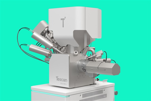
Tescan Solaris X 2- xenon plasma FIB for advanced packaging. Tescan