
Leading semiconductor test equipment supplier Advantest Corporation (TSE: 6857, NYSE: ATE) announced that a new mold thickness metrology system, the TS9000, for measuring the thickness of semiconductor packaging, is available for purchase. The system is based on advances in Terahertz (THz) technology pioneered by Advantest.
The TS9000 Mold Thickness Analysis (MTA) System is a new metrology tool that performs non-destructive analysis of the thickness of semiconductor packaging. Meeting the high standards of speed and accuracy required for high-volume manufacturing, its innovative inspection capabilities are expected to contribute significantly to product quality improvement amid the trends towards smaller device sizes and higher integration, driven in part by the widespread adoption of smartphones and tablets.
Already installed and in use, the TS9000 heralds a new product family of analysis systems for high-volume manufacturing. Future systems from the THz product family will target the pharmaceutical, automotive, ceramic and other industrial markets in addition to semiconductors. Advantest is leveraging its leading capabilities in terahertz technology to bring cutting-edge non-destructive analysis to industrial production lines.
Background
The worldwide embrace of smartphones and other advanced consumer electronics is driving demand for smaller, more highly integrated semiconductor devices. Semiconductor packages for this market must be compact, thin, and tough enough to stand up to mobile usage. The semiconductor industry has few higher priorities than achieving an optimal balance of package durability and thinness.
However, existing metrology methods are not suitable for volume production lines. Manufacturers have had to test package thickness by inspecting samples late in the production process. Existing metrology methods are slow, laborious and destructive and not compatible with quality control in a high volume environment. This makes it difficult to assess the quality of the entire production run and problematic to trace the root cause of any defects in the final product.
Advantest's TS9000 solves these issues by enabling rapid, repeatable, and highly accurate measurements of mold thickness, without the limitations of existing measurement methods. Highly adaptable, it can be deployed at various points in the assembly and packaging process, even immediately after the curing process, enabling earlier detection of production issues and improving product quality and yield.
Product Features
*Non-Destructive Terahertz Technology: The TS9000 exploits the unique characteristics of terahertz radiation, which have high penetration into many materials, including ceramics, silicon and plastic polymers, even if those materials are optically opaque. This allows for non-destructive layer thickness measurements in a wide variety of materials.
*Suitable for High Volume Manufacturing Environments: Advantest's proprietary technologies, such as rapid fiber coupled pulsed laser generation and detection of THz waves, enable the TS9000 to meet the highest industry standards for measurement speed and accuracy. This first-in-class system delivers throughput suitable for a high-volume manufacturing environment.
*Improved Quality Control: The TS9000 can be implemented early in the process and be used to measure strip packages - before units are cut into single devices. This, coupled with the significantly higher throughput compared to conventional mold thickness measurements, makes this a tool which can drastically improve process quality control.
*Diverse Form Factors: In addition to strip units, the highly adaptable TS9000 supports measurement of individual devices handled using industry standard JEDEC trays, making it flexible and compatible with existing sample handling methods.
Key Specifications
Application: Semiconductor package thickness inspection
Measurable Layer thickness: 30μm ~ 600μm
Accuracy: better than 3μm
Operating environment: Temperature: +10 degrees C ~ +30 degrees C; humidity: <80%
Dimensions: Analysis unit: 430 (W) × 540 (D) × 330 (H) mm / 30 kg or less
Optical unit: 430 (W) × 240 (D) × 220 (H) mm / 14 kg or less
Measurement unit: 1050 (W) × 650 (D) × 450 (H) mm/67kg or less
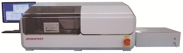
TS9000 measurement unit (left), controller (right), and analysis software screenshot (rear).
DIGITIMES' editorial team was not involved in the creation or production of this content. Companies looking to contribute commercial news or press releases are welcome to contact us.

