![]()
Tuesday 2 June 2026
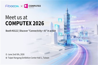
Fibocom Showcases at COMPUTEX 2026: Accelerating 'Connectivity + AI' in High-Value Scenarios
At COMPUTEX 2026, Fibocom outlined its perspective on the deployment path of edge AI: as AI moves from the cloud to end devices, the key to large-scale adoption lies not only in model performance, but also in the synergy between stable connectivity and local computing power.Based on this insight, Fibocom continues to strengthen its "Connectivity + AI" capability. On one hand, with wireless modules at its core, Fibocom has built a connectivity product portfolio covering FWA, AI CPE, and next-generation Wi-Fi 8, providing a high-speed, low-latency, and highly reliable connectivity foundation. On the other hand, by leveraging its full-stack AI solutions, Fibocom enhances on-device AI capabilities, enabling terminals with local perception and processing power to improve the stability and responsiveness of AI applications in complex environments.For intelligent edge scenarios, Fibocom launched the Fibocom ClawBox, a high-efficiency AI computing terminal natively compatible with intelligent agents such as OpenClaw and Hermes Agent. Built on a high-performance heterogeneous computing architecture, the product integrates CPU, GPU, and NPU, delivering up to 18 TOPS @ INT8 hybrid precision computing power. With typical power consumption at around 5W, it enables high-density, multi-task parallel inference. It supports multi-stream video analytics, complex visual structuring, voice, and multimodal model inference, while offering low latency, high reliability, and localized deployment capabilities. Combined with Fibocom's Skill Hub, it is widely applicable in security, transportation, robotics, and other intelligent edge scenarios, supporting the large-scale deployment of smart industry applications.At COMPUTEX 2026, Fibocom will showcase a range of innovations at Booth K1022, including AI companion solutions, robotic lawn mower solutions, mobile robotics solutions, and more, demonstrating how "Connectivity + AI" is creating value in high value scenarios. Industry partners are warmly welcome to visit and connect with us.