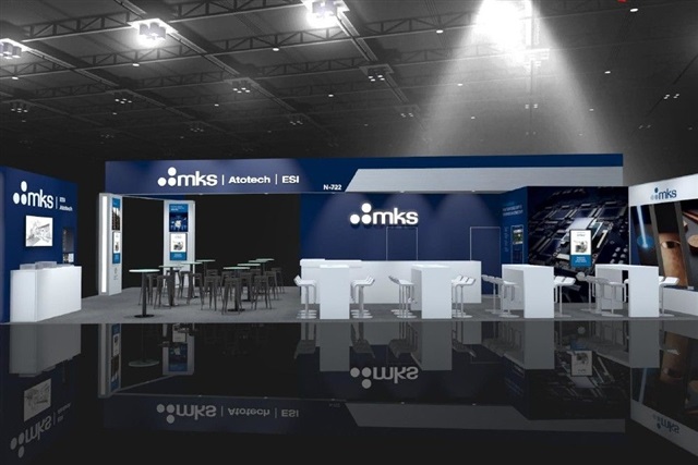
MKS Inc. (NASDAQ: MKS), a global provider of enabling technologies that transform our world, today announced that its strategic brands Atotech, offering process chemicals, equipment, software and services, and ESI, providing laser systems, will showcase advanced manufacturing solutions for printed circuit boards (PCBs) and package substrates at TPCA Show 2026. The event will take place at the TaiNEX Center in Taipei, Taiwan, from October 20 to 22, 2026.
Enabling Next-Generation Electronics Manufacturing
The next phase of PCB manufacturing is defined by more than just design capability; it is also defined by the ability to reproduce advanced structures in large quantities with a stable yield and reliable performance. As high-layer-count multilayer and HDI PCBs transition to finer features, thinner dielectrics, and tighter assembly margins, achieving manufacturing consistency becomes paramount. In these circumstances, surface condition, seed layer and copper deposit quality, as well as final finish stability directly affect production yield and downstream performance.
As AI and HPC architectures increase interconnect density, bandwidth, and power delivery demands, PCB manufacturers must supply more advanced high-layer-count multilayers, HDI, substrate-like PCBs, and package substrates that meet tighter consistency requirements. In that environment, manufacturing becomes a determining factor in whether next-generation interconnect structures can be produced with acceptable yield, reliability, and assembly performance.
At TPCA Show 2026, MKS will present integrated surface treatment, laser processing, metallization, plating and final finishing chemicals and systems technologies for high-density PCBs, advanced package substrates, optical modules and next-generation packaging architectures.
By integrating MKS' ESI laser systems with Atotech's advanced chemistry and plating equipment, MKS delivers a comprehensive, one-stop solution for electronics manufacturing. This unified approach combines optimized laser drilling, plating, and surface modification chemistries with state-of-the-art equipment - enabling seamless pre-treatment, via formation, plating, and final finishing.
This innovative approach results in improved yields, enhanced productivity, and superior performance - all without production interruptions.
"As AI, high-performance computing, and advanced packaging reshape the electronics industry, the challenge is no longer simply creating smaller features or denser interconnects, but manufacturing increasingly sophisticated structures reliably, consistently, and at scale. Industry leadership depends not only on design innovation, but on controlling every critical interface across surface preparation, metallization, copper deposition, and finishing. As the boundaries between semiconductors, substrates, packaging, and PCBs blur, the reliability and efficiency of tomorrow's AI infrastructure will increasingly depend on an integrated approach that optimizes materials, chemistry, equipment, and process control as a complete manufacturing ecosystem." Dave Henry, Executive Vice President & GM of Materials Solutions Division, MKS.
In 2026, MKS' Atotech is driving innovation in advanced electronics manufacturing through strategic investments in its Asia-based technology centers. These enhancements accelerate development for next-gen package substrates and support high-end SAP applications with line/space requirements of ≤5/5µm.
"In partnership with industry leaders, MKS' Atotech is advancing technology for substrate-like PCBs, advanced high-layer count HDI and multilayer for AI PCBs and optical modules. By bringing together expertise in materials, chemistry, and systems technologies, we are enabling the next generation of electronics while driving innovation, performance, and manufacturing integration across the industry," said Harald Ahnert, Senior Vice President and General Manager of Chemistry at MKS' Materials Solutions Division.
Bonding Enhancement: Improving Signal Integrity Without Compromising Adhesion
AI, high-performance computing, and high-frequency applications demand strong copper-to-dielectric adhesion with minimal surface roughness, to address rising data throughput requirements. MKS' Atotech addresses this challenge with its I/L bonding portfolio, including BondFilm HF, BondFilm EX, and NovaBond PX-S2. These solutions are designed to provide reliable bonding while limiting copper roughness and line-width distortion, helping reduce conductor loss and preserve circuit geometry. By supporting low-loss dielectric materials, the portfolio helps PCB, HDI, and package-substrate manufacturers improve signal integrity while maintaining the adhesion required for reliable next-generation electronics.
Desmear and Metallization: Building a Reliable Foundation
Reliable interconnect formation begins with high-quality desmear and metallization. As vias become smaller and dielectric materials more diverse, consistent metallization is critical to ensuring long-term performance and yield. MKS' Atotech metallization solutions are engineered to deliver uniform coverage, strong throwing power, and defect-free copper deposition across advanced substrates, HDI designs, and AI-driven PCB architectures. The Printoganth MV TP3 family supports ultra-thin electroless copper deposition and, when combined with the innovative G-Plate platform, enables advanced particle control for high-volume manufacturing. Printoganth P2 is designed for demanding AI, HDI, and multilayer board applications, while Cupraganth MV Activator provides an alternative to palladium-based activation for IC substrates. Together, these technologies provide the robust process foundation required for increasingly complex electronics manufacturing.
Electrolytic Copper Plating: Optimized for High-Volume Manufacturing
In advanced PCB and substrate manufacturing, consistent plating performance at production scale is essential. MKS' Atotech combines its production-proven Inpulse chemistry portfolio with Uniplate equipment to deliver highly controlled copper deposition processes that enhance yield, reduce variability, and ensure reliable feature filling across challenging designs Solutions including Inpulse 2HFU2, Inpulse 2HT, and the Cuprapulse series provide superior conformal coverage, high throwing power and uniform copper distribution. Inpulse 2HF9 and InPro THF2 provide superior microvia filling and uniform copper distribution. For next generation package substrate build-up layers, InPro SAP7 provides best copper distribution at high current densities. The integrated approach of our Uniplate PLBCu lines helps manufacturers achieve the reliability, scalability, and process consistency required for next-generation AI, HPC, and advanced packaging applications.
Final Finishing: Protecting Performance Through Assembly and Beyond
The final surface finish plays a critical role in ensuring assembly success, long-term reliability, and overall manufacturing efficiency. MKS' Atotech offers a comprehensive portfolio of industry-leading finishing technologies that protect copper from oxidation, maintain excellent solderability and bondability, and support increasingly fine-feature designs. The latest Stannatech 2100 and Stannatech IC immersion tin solutions deliver enhanced solderability, lower ionic contamination, and compatibility with advanced substrate applications. For ENIG, ENEPIG, and EPAG processes, MKS combines Aurotech NIC electroless nickel, PD-Core electroless palladium, and Aurotech G-Bond 3 gold technologies to provide high-quality finishes with reduced precious metal consumption, short cycle times, and exceptional process robustness. These solutions help manufacturers maximize assembly yields while meeting the performance requirements of next-generation electronics.
Systems Solutions: Driving Integrated Systems Precision at Every Stage
PCB equipment system highlights include G-Plate, a new high-volume manufacturing (HVM) platform for PTH processing of next-generation package substrates, enabling highest yields and supporting cutting-edge fine-line capability targeting L/S < 5/5 µm. The portfolio further includes vPlate, a new vertical continuous plating system for advanced HDI, optical module, and package substrate applications, delivering best-in-class surface uniformity and optimized for mSAP pattern plating. Uniplate, the company's flagship HVM platform and industry-leading horizontal plating solution, serves next-generation HDI PCB, optical module, and package substrate manufacturing, including mSAP panel plating applications. Complementing these systems is the Polygon PLBCu Line, engineered for superior blind microvia (BMV) filling and high aspect ratio through-hole (TH) plating, enabling robust HDI and MLB production and supporting demanding applications such as AI server boards.
Laser equipment promotions include the latest Capstone, a high-performance/throughput breakthrough productivity for flex PCB UV drilling and Geode platform (CO2 and UV laser for HDI and package substrate applications). A special show highlight Geode A a new CO2 laser system for high precision and high-speed ABF build-up laminate processing. Geode G2 the new CO2 laser system for high-precision and high-speed HDI and mSAP via drilling. The Geode platform provides increased productivity, the smallest footprint, and the lowest power consumption in the market.
Glass Technology: Next-Generation Advanced Packaging Technology
Not only displaying the glass sample, but a set of PoG 3D models is on the stage. MKS' Atotech and AUO Corporation will showcase their Glass Core Substrate (GCS) technology at the MKS booth. The glass sample integrates AUO's large-size glass processing, precision metallization, and redistribution layer capabilities, and is advancing glass vias, hole metallization, and reliability verification in stages with VitroCoat GI, Cupratech GIM, Inpro Pulse TGV and EcoFlash. Compared to traditional substrates, it is more suitable for next-generation advanced packaging technologies such as AI, HPC (high-performance computing), HBM (high-bandwidth memory), and CPO (co-packaged optics), helping to improve system performance and energy efficiency. The PoG 3D models are made with 3D printing technology to demonstrate the structures and different layouts of glass core and glass interposer technology. By disassembling the models and looking at the glass sample, visitors will understand more about the most advanced technology in the world today. Also, the difficulties to achieve this task to try and find out solutions for it. In the meantime, MKS sponsors an IMPACT session to discuss glass technology in more depth with 5 experts in the field.
"We are proud to continue our partnership with IMPACT and host this year's Industrial Forum, 'Enabling AI and HPC: Technology Inflections Across Advanced Packaging and Interconnect.' As AI infrastructure advances, we are focused on enabling next-generation chip packaging, package substrates, and high-performance interconnects. Across the IMPACT Conference and Tech x Total Solution Seminar, MKS' strategic brands Atotech and ESI will showcase integrated process and equipment innovations that help customers meet the growing demands of AI-driven electronics manufacturing," said Wayne Cole, Senior Vice President, Global Sales of Materials Solutions Division, MKS.
For more information please visit: TPCA Show 2026 and IMPACT-IAAC 2026.
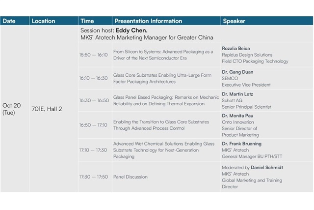
MKS Atotech Features Glass Core Substrate Expertise at IMPACT 2026. Credit: MKS-Atotech
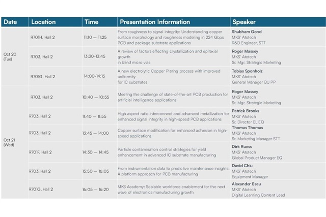
MKS Atotech Experts Share Technical Insights at IMPACT 2026. Credit: MKS-Atotech