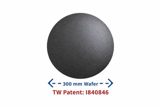
As AI, high-performance computing (HPC), and advanced packaging continue to move toward higher levels of power integration, chip power consumption is rising rapidly. Thermal management has therefore become a critical factor affecting performance, reliability, and system design. World Diamond Technology is advancing its large-area diamond growth technology and accelerating the mass production of 300 mm diamond wafers to address the thermal management needs of AI chips and advanced packaging.
Five Key Priorities for Mass Production
The 300 mm wafer is currently the mainstream format in advanced semiconductor manufacturing. Scaling diamond materials from conventional smaller sizes to 300 mm involves far more than simply increasing the surface area. It also presents multiple technical challenges related to large-area material processing, uniformity, thickness, flatness, internal stress, and surface quality.
World Diamond Technology has continued to advance its large-area diamond growth technology and has secured a Taiwan patent (TW Patent: I840846). Its mass-production strategy focuses on five key priorities:(1)Optimizing the diamond growth process through proprietary WDCVDTM diamond growth technology to ensure consistency across large-area wafers.(2)Precisely controlling wafer thickness and uniformity to meet the stringent requirements of advanced packaging thermal management modules.(3)Strengthening flatness and internal stress management to improve yield and reliability.(4)Optimizing surface quality and process consistency to minimize defects.
(5)Continuously improving production yield and capacity while establishing a stable supply chain to support customers' volume-production requirements.
By advancing toward the 300 mm format, World Diamond Technology aims to increase the potential for integrating diamond materials with existing semiconductor processes and wafer-level application platforms, enabling diamond to progress from a specialty material toward large-scale adoption across the semiconductor industry.
Advantages of Diamond Materials
Diamond offers multiple advantages as a thermal management material. Its thermal conductivity can exceed 1,500 W/(m·K), significantly outperforming conventional heat-dissipation materials. Diamond also features an extremely low coefficient of thermal expansion, helping substantially improve device reliability.
In addition, diamond delivers exceptional hardness, wear resistance, high-temperature durability, and chemical stability. These properties enable it to resist corrosion, operate reliably in high-temperature environments, extend product service life, and reduce the total cost of ownership.
Targeting AI Chips and Advanced Packaging Applications
World Diamond Technology's 300 mm diamond wafers will focus on high-power, high-heat-flux semiconductor applications, including:(1)AI GPUs and HPC systems(2)Data centers and servers
(3)2.5D and 3D advanced packaging(4)High-power laser devices(5)Automotive electronics and power modules
As advanced packaging architectures become increasingly complex, thermal management is evolving from conventional system-level cooling toward package-level, device-level, and even wafer-level solutions. Consequently, the importance of high-thermal-conductivity materials will continue to grow.
Diamond Technology Powering a High-Efficiency Future
World Diamond Technology stated that the 300 mm diamond wafer represents an important milestone in the company's efforts to industrialize large-area diamond materials. In the next phase, the company will continue to focus on process stabilization, yield improvement, specification standardization, customer validation, and the establishment of volume-production capabilities. It will also actively pursue collaboration with semiconductor manufacturers, advanced packaging companies, thermal module suppliers, and end-system providers.
To meet the rapidly growing thermal management demands of the AI era, World Diamond Technology will continue to advance diamond materials from material development to practical semiconductor applications. The company is accelerating the establishment of a comprehensive technology portfolio spanning diamond wafers, diamond lids, diamond heat spreaders, and system-level thermal management solutions, positioning itself to capture opportunities in the next generation of high-power chips and advanced packaging.
Discover the latest developments in diamond wafer technology at SEMICON Taiwan 2026. We cordially invite you to visit World Diamond Technology at Booth S7546 on the 4th floor of Taipei Nangang Exhibition Center, Hall 2.