
CONNECT WITH US
Sign out

TSMC's refusal of ASML's expensive High-NA EUV equipment, explained

, Hsinchu
0

Credit: DIGITIMES

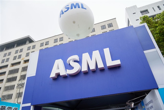
ASML has launched its 0.55 High Numerical Aperture Extreme Ultraviolet (High-NA EUV) in an effort to extend Moore's Law. The market had originally expected TSMC to adopt it first, but the company has held back. TSMC Senior Vice President of Global Business Kevin Zhang stated at the North America Technology Symposium that there are currently no plans to introduce High-NA EUV before 2029, mainly because "it's too expensive!" This decision also reflects how TSMC is shifting competition focus from equipment to process integration and cost efficiency.

ASML's next-generation High-NA EUV equipment was unexpectedly first adopted by Intel, while Samsung Electronics has also expanded procurement, yet TSMC has taken the opposite approach. According to plans made between TSMC and ASML several years ago, High-NA EUV was originally expected to be introduced in the A14 node around 2028. However, after multiple rounds of discussions over the past two years, TSMC Chairman C.C. Wei led senior executives to visit ASML's headquarters in the Netherlands in mid-2024, with both sides even publicly sharing photos of the visit.

Half a year later, ASML's CEO personally visited Taiwan to meet TSMC, but pricing negotiations still failed. Each High-NA EUV system costs as much as EUR350 million (approx. US$410.3 million). Given the high R&D costs, if ASML were to concede on pricing, other customers would likely demand similar discounts.

TSMC's strengths

TSMC holds three key advantages that give it the upper hand. According to Zhang, the primary reason is that TSMC continues to strengthen the technical capabilities of its existing EUV equipment, allowing it to further shrink chip sizes and improve performance. The company has been cautious towards High-NA EUV for a long time. At its 2024 and 2025 technology forums, the company already indicated that its A16 and A14 nodes would not adopt High-NA EUV.

Now, the timeline has been further delayed. According to its latest roadmap, the A13 node planned for mass production in 2029 can still achieve about a 6% area reduction compared to A14 without relying on High-NA equipment.

High-NA EUV does represent a leap in lithography technology. Compared with 0.33 NA systems, 0.55 NA High-NA EUV can improve resolution, deliver higher image contrast at the same chip size, reduce required exposure energy, and shorten per-layer printing time, thereby boosting fab productivity. However, the current price of a single High-NA EUV system is nearly double that of existing EUV equipment.

Its introduction would also trigger a restructuring of the process ecosystem, including higher mask costs, development of next-generation photoresists, increased power consumption, and more complex maintenance requirements. The sharp rise in power usage has already become a headache for TSMC, while depreciation periods for such expensive equipment would also lengthen.

TSMC's capital expenditures are expected to approach US$56 billion in 2026 and remain elevated in the coming years. Entering the High-NA EUV era would push capex even higher. For TSMC, delaying adoption is a positive choice for profitability. Aside from cost pressures, the technical risks of adopting High-NA EUV are also significantly higher, and next-generation photoresist materials are still under optimization.

Three risk factors for High-NA EUV adoption

TSMC will not proceed hastily until these risk factors are resolved. In addition, TSMC has already demonstrated that it can deliver competitive performance, power, and area (PPA) using existing technologies. For customers, whether High-NA EUV is adopted is not critical. In fact, if introduced, TSMC might need to raise prices to pass on higher production costs.

One of TSMC's key advantages in saying no to ASML lies in its long-developed in-house EUV pellicle, now assigned to its upgraded 8-inch Fab 5 in the Hsinchu Science Park (HSP). Compared with traditional deep ultraviolet (DUV) equipment, EUV systems require further adjustments in masks and pellicles. The pellicle has always been a critical protective mechanism in semiconductor processes to prevent particle contamination. The organic pellicles widely used in the past are no longer suitable due to limitations in transparency and stability. Most modern EUV processes use pellicle-free masks, requiring frequent inspections.

If defects are found, masks must be repaired or remade, significantly increasing production costs and reducing speed. TSMC believes EUV pellicles are crucial for improving efficiency and lowering costs in sub-7nm processes, and has accelerated in-house development for years. Compared with competitors that rely heavily on ASML's EUV equipment to advance processes, TSMC's in-house pellicle allows it to further optimize existing processes and gain cost advantages.

The second factor is advanced packaging and system integration. The focus of performance improvement is shifting from single-chip scaling to multi-chip packaging and system integration. Wei previously stated that relying solely on chip technology is no longer sufficient to meet AI performance demands. Future advancements will be driven by system-level innovation.

TSMC is actively advancing technologies such as CoWoS, InFO, SoIC, and CoPoS, as well as adopting chiplet architectures. This allows system performance improvements without relying entirely on transistor scaling, while also expanding into COUPE silicon photonics technology.

The third factor is TSMC's dominance in the foundry industry, including its customer base, capacity, and profitability. As competitive barriers rise, Samsung and Intel have invested heavily in High-NA EUV to surpass competitors through advanced equipment. However, this strategy may instead weigh on their profitability. Without sufficient order volumes to support these investments, the massive capital expenditures for new fabs and equipment depreciation may take a long time to recover.

If yields do not improve, adopting High-NA EUV could further strain the financial positions of Samsung and Intel. TSMC's wait-and-see approach has ultimately become its greatest advantage.

The pressure now shifts back to ASML. Although ASML remains confident about the future, it will lack major High-NA EUV orders from TSMC over the next three to four years, while the Chinese market continues to shrink. For now, orders from logic and memory customers expanding production are still providing support. However, if the memory industry stabilizes and Samsung and Intel also reassess and follow TSMC in delaying High-NA EUV purchases, ASML's operations could face a significant impact.

Article translated by Emily Kuo and edited by Jack Wu