
According to news reports, Samsung and TSMC are expected to enter 5nm process mass production in 2020. The competition in 5nm wafer yield and market share will be very intense. A brand new wafer defect analysis platform featuring two crucial technologies - namely "smart defect screen and sample technology" and "defect size metrology technology" - can discover various types of tiny yield loss defects in 5nm process and enhance 5nm wafer yield.
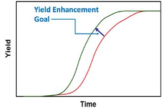
To win 5nm race, you need to know what is the most critical factor
Fab engineers know for a fact that discovery of bad defects in 5nm process is much more difficult than in 12nm process. In the race of 5nm wafer yield, the defect analysis technology in the inline wafer inspection must be improved. The wafer yield improvement process is described in the following steps. Step 1: Defect inspection -> Step 2: Defect analysis platform selects bad defect for sampling -> Step 3: Take bad defect samples' SEM images through Review SEM -> Step 4: Root cause analysis of bad defects. Since bad defects directly impact wafer yield. The discovery of bad defects is dependent upon the defect analysis platform in step 2. Then, the fab is able to dig out root causes of bad defects and improve yield afterward. So, the most critical factor in winning 5nm wafer yield is the capability of defect analysis platform.
Critical know-how to improve 5nm wafer yield - Defect size metrology technology
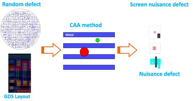
Very often fab suffers big issue in discovering bad defects in advanced technology. ESI's invention patent, Method for smart defect screen and sample, which maps inline defect to corresponding IC design layout and performs Critical Area Analysis to classify nuisance defect and killer defect. The breakthrough of this smart defect screen platform can identify and filter most of nuisance defects accurately. The basic concept in ESI's invention is "The more nuisance defects to be filtered accurately, the more bad defects to be discovered." This accomplishment makes ESI's defect patent invention technology the best in the world.
To meet the more advanced 5nm and 3nm process challenges, ESI already finished the development of defect size metrology technology and patent portfolio. Nuisance defects are falsely classified into killer defects because of incorrect defect size measurement results. ESI's defect size metrology technology successfully improves wafer yield by providing correct defect size.
ESI OpenShort Platform, including smart defect screen and sample technology and defect size metrology technology, has distinguished itself in the race for 5nm win.
The best smart inline defect analysis platform - ESI OpenShort Platform
No doubt the smart defect analysis platform is a prime and must selection tool for yield enhancement in semiconductor industry. After the detailed prior art search, Gainia Inc., the intelligent asset services at ITRI, pointed out that ESI's patent invention "Method for smart defect screen and sample (US 8312401, CN1614876, ROC I402928)" is the founder of Artificial Intellegence defect analysis in the world. Based on that invention, ESI OpenShort Platform is one of a kind in the industry.
More information about Elite Semiconductor, please invist: http://www.elitesemi.com.tw/
OpenShort Platform
OpenShort Platform
DIGITIMES' editorial team was not involved in the creation or production of this content. Companies looking to contribute commercial news or press releases are welcome to contact us.

