electronics as the basis for the All Electric Society
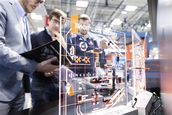
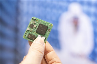
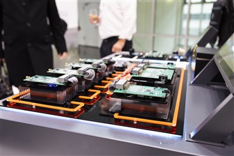
Whether it's speech and object recognition, image classification, predictive maintenance, or autonomous control, Artificial Intelligence (AI) applications require powerful electronic systems. It is only modern semiconductors and sensors, scalable embedded systems, and efficient connectivity that enable AI solutions in industry, mobility, energy, and medicine in the first place. At the same time, as the use of AI grows, so do the demands on computing power, energy efficiency, and cyber resilience. The electronics industry will show which technologies are driving this development at electronica in Munich from November 10 to 13.The electronics industry provides the technological basis for the All Electric Society and enables intelligent applications in energy supply, mobility, industrial automation, and buildings. "Artificial Intelligence places whole new demands on electronic systems. What's needed are powerful, energy-efficient, and secure solutions in which hardware, software, and connectivity work together seamlessly," says Caroline Pannier, Exhibition Director for electronica. "It's precisely these developments that are the focus of electronica." AI as an accelerator and stress test for the economy and infrastructure.?AI as an accelerator and stress test for the economy and infrastructureTo remain innovative and competitive, companies today must integrate AI into their products, services, and processes. According to the German Economic Institute, 66.3 percent of large companies are already using AI, while about half of medium-sized companies are doing so. Small businesses have the most ground to make up: Only 35.6 percent use AI in their operations.At the same time, AI is opening up entirely new possibilities: machines and vehicles are becoming smarter, energy grids more efficient, medical diagnoses more accurate, and devices more autonomous. However, as the use of AI grows, so do the energy needs and cybersecurity requirements.Energy efficiency and cyber resilience as key criteriaDue to the increased use of AI, modern electronic systems must provide high computing power, use energy sparingly, and operate reliably under thermal conditions. At the same time, the attack surface for cyber risks grows as systems that exchange large amounts of data become increasingly connected, and software updates are released regularly.As a result, energy efficiency and cyber resilience are evolving from individual, isolated requirements into core system criteria. In addition, the EU Cyber Resilience Act (CRA) increases the pressure on companies to take action. Approaches such as "security by design" must therefore be incorporated as early as the architecture phase and integrated across hardware, software, interfaces, updates, and operating concepts.Hardware, software, and the application layer are convergingThe development of modern electronics is increasingly shifting from optimizing individual components to integrated, complete systems. What matters is no longer just the performance of an individual processor, sensor, or module, but rather the interaction between hardware and software, the operating system, connectivity, security, and the application layer. Customers expect products that can be quickly integrated, easily scaled, and updated throughout their lifecycle. This places greater demands on system design, software quality, and lifecycle management. At the same time, that opens up opportunities for the electronics industry to tap into new markets and make itself competitive for the future.electronica as a platform for AI, cyber resilience, and energy efficiencyAs the world's leading trade fair for electronics, electronica brings together key players that cover the entire spectrum of the industry. Around 3,500 exhibitors from some 60 countries will show how individual components are transformed into integrated, intelligent, and secure complete systems. The focus will be on the key topics of Artificial Intelligence, energy efficiency, and cyber resilience. An extensive supporting program will provide for further discussion and knowledge sharing. SEMICON Europe, taking place in parallel across two and a half halls, will offer insights into the entire semiconductor industry value chain.