

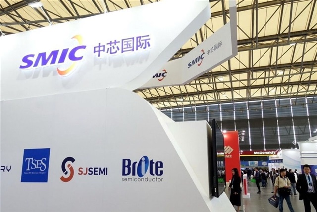
China-based foundry SMIC will release fourth-quarter 2025 results on February 10 and hold its first 2026 investor briefing on February 11. Market focus is expected to center on its advanced packaging push, which is shifting from a supporting function toward a core manufacturing strategy.
At the end of January, SMIC inaugurated its Advanced Packaging Research Institute in Shanghai, led by chairman Liu Xunfeng. Although the company has not disclosed detailed plans, policy alignment and government-backed resources have led the market to interpret the move as a structural repositioning of back-end and midstream manufacturing capabilities rather than a standalone technical project.
With leading-edge process scaling facing structural limits and demand rising for AI and chiplet architectures, advanced packaging is increasingly viewed as a primary path to extend performance and system integration. SMIC's renewed focus reflects the changing competitive logic of the post-Moore era.
Two decades of manufacturing strategy resets
SMIC's advanced packaging strategy dates back more than two decades. During its early formation, founder Richard Chang promoted vertically integrated manufacturing, combining wafer fabrication, packaging, and testing to accelerate volume production and strengthen access to global supply chains.
The strategy soon faced operational and external pressure. Profitability remained weak for extended periods while external challenges intensified.
Between 2003 and 2009, patent and trade secret disputes with TSMC became defining events in SMIC's history. Prolonged litigation created financial and reputational pressure while increasing scrutiny across equipment procurement, technology partnerships, and customer relationships. Operating multiple adjacent businesses under these conditions was widely viewed as increasing operational risk.
In 2009, SMIC initiated strategic retrenchment by spinning off packaging and testing operations into Siltech, allowing resources to refocus on core foundry operations. The move was widely viewed as operational stabilization under legal and capital market pressure rather than a rejection of packaging value.
Packaging emerges as primary performance path
As process scaling approached physical and cost limits, the traditional node-driven growth model weakened. Around 2014, SMIC established a 3D IC Division to restart systematic research into advanced packaging and 3D integration. The move reflected internal recognition that future performance gains would increasingly come from packaging architecture and system-level design rather than transistor scaling alone.
During the same period, SMIC partnered with JCET to form SJ Jiangyin (SJ), focusing on midstream processes, including 12-inch wafer bumping and redistribution layer (RDL) technologies through a relatively independent platform. In 2016, SJ achieved volume production of 14nm wafer bumping, marking a milestone for China's advanced packaging ecosystem.
Export controls drive structural supply chain separation
After 2018, external conditions shifted again. US export controls and investment restrictions expanded beyond leading-edge equipment to include EDA tools, supply chain relationships, and corporate equity structures. Under these conditions, joint ventures closely tied to foundry operations and advanced packaging drew increased regulatory and market scrutiny.
Between 2017 and 2019, SMIC transferred specialty process assets to SMEC (now United Nova Technology), while gradually moving packaging and midstream assets into SJ to create a clearer separation between wafer manufacturing and packaging pathways. In 2021, SMIC sold its remaining SJ stake, completing capital-level separation. SJ was later renamed SJ Semiconductor Corporation (SJ Semi).
Industry interpretation has been consistent: the restructuring was a risk management adjustment under intensifying US–China technology tensions, not a withdrawal from advanced packaging strategy.
Chiplet and advanced packaging strategy gain internal traction
SMIC's long-term advanced packaging strategy remained intact through these structural shifts. At the end of 2020, TSMC co-COO Chiang Shang-yi joined SMIC and emphasized that advanced packaging combined with chiplet architecture would drive computing performance growth in the post-Moore era.
He also proposed manufacturing models integrating mature process nodes, heterogeneous integration, and system-level production. Although related programs later slowed under multiple constraints, the technical roadmap left a lasting strategic imprint inside SMIC.
AI demand accelerates system-level integration shift
With multiple twelve-inch fabs expected to enter SMIC's production system around 2026, AI and high-performance computing demand are expanding across advanced packaging, chiplet integration, and system-level assembly. Advanced packaging is again moving toward the center of SMIC's manufacturing strategy.
From Richard Chang's integrated manufacturing vision, through litigation-driven retrenchment, to structural rebuilding under geopolitical pressure, SMIC's advanced packaging path has been complex. It reflects continuous strategic recalibration under constrained conditions.
As the post-Moore era accelerates, advanced packaging is returning to the center of the semiconductor value chain.
Article translated by Levi Li and edited by Jack Wu
