
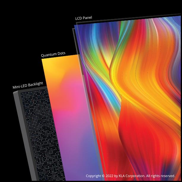
MiniLED is an up and comer in the displays category, particularly for tablets, TVs and gaming monitors. This relatively new technology, used for backlighting LCD displays, offers deeper blacks, improved contrast ratios and brighter panels, compared to traditional LED-backlit LCD technology. But there is a challenge that looms as miniLED moves into mass production: miniLED backlight units require a substrate – either PCB or glass – covered with white solder mask. Why does the manufacturing process with white solder mask present a challenge? To better understand, let's look at the benefits of miniLED, why white is the preferred solder mask, and the resulting manufacturing challenges.
According to an Omdia report, "OLED and LCD Supply Demand & Equipment Tracker – 2Q21 Analysis," shipments of LCD panels with miniLED backlights are expected to grow from 9.7 million units in 2021 to 37.9 million units in 2025. More specifically, TVs and tablets are the leading miniLED applications, with significant growth predicted for TVs through 2025. The use of miniLED for notebook PCs is also gaining traction and predicted to increase in volume during the same period. MiniLED is becoming a popular choice for OEM designers because it provides better contrast, richer colors and improved image quality, and can be a cost-effective alternative to OLED.
OLED vs. miniLED
OLED is a popular technology, with self-luminous displays and panels that do not require a backlight unit due to their light-emitting characteristics. OLED can provide better color contrast than miniLED, but it is often quite expensive and there are some disadvantages in lifespan and performance in outdoor environments. MiniLED, on the other hand, has excellent brightness, reduced energy consumption, high refresh rate and a wide color gamut with less design complexity. As a result, many of the largest TV, tablet and notebook manufacturers are eager to adopt miniLED technology since it offers quality and other improvements over standard LED technology and is more cost effective than OLED.
To provide all these benefits, the solder mask exposure process for miniLED-based devices requires high accuracy and yield. Manufacturers must be able to achieve superior accuracy to meet the demanding specifications of miniLED-based products, as required by the designers. Direct imaging (DI) for the solder mask exposure process is an ideal solution for this because it enables high accuracy, while overcoming challenges such as panel topography, distortion and fine features, all of which can influence product quality and yield.
MiniLED backlight unit on a large-size TV
Advantages & Challenges of White Solder Mask for miniLED
Designers of miniLED BLU (backlight units) devices typically require that the substrates manufactured by their supply chain will be covered with white solder mask, which has a very high reflectivity rate (>90% in many cases). This enables the high contrast and brighter colors that deliver a sharper image on TVs, tablets and notebooks/PCs. All these substrates, whether PCB or glass, are produced with openings to receive the miniLED chips in the next stage of assembly, either package on board (POB), chip on board (COB) or chip on glass (COG). Highly accurate and uniform opening dimensions are critical to the quality of the miniLED end-product.
There are three factors in the white solder mask DI exposure process that can create challenges for manufacturers: the first is accuracy, the second is quality and yield, and the third is capacity which also translates to cost.
MiniLEDs range from 50 to 300 microns in size, and they must be positioned very accurately, with an extremely small standard deviation. For example, the uniformity of the solder resist openings (SROs) on the substrate cannot deviate more than ±5 microns for some applications. High-end devices typically require higher accuracy. Achieving such strict registration accuracy is even harder when the panel targets are covered with thick white solder mask, and a special illumination or sophisticated algorithm is required to acquire the target position with high accuracy.
Quality is the second challenge, relating to uniformity of the solder resist openings and to strict undercut requirements. The white solder mask used for miniLED production scatters most of the illumination wavelength, so the exposure UV light is not absorbed as it would be with other solder mask colors, resulting in an inferior solder mask polymerization process. An undercut is formed when the bottom part of the solder mask layer is not fully polymerized during the exposure process. This may lead to the possibility of a peel off. Severe undercut (see image below) is often problematic for miniLED manufacturers. Minimal undercut (see image below), which creates robust dams, is a requirement for high quality and high yield. The creation of robust dams with minimal undercuts requires the use of an optimized wide range of illumination wavelengths in the exposure process, to expose the reflective, thick white solder mask.
To address cost, manufacturers of PCB or glass substrates for miniLED devices need to maximize production capacity and optimize their cost per print. This can most easily be achieved by using a high throughput solution that also addresses the unique challenges of white solder mask exposure mentioned above.
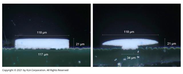
Left: White solder mask dam with minimal undercut. Right: White solder mask dam with severe undercut
What's next?
As demand for miniLED-based consumer electronics increases, new and innovative advanced solder mask exposure methods are needed to meet high accuracy, quality and capacity requirements. Direct imaging solutions that overcome the challenges of white solder mask exposure are necessary for manufacturers to produce high-quality substrates at mass-production levels to meet rising demand for tablets, TVs, gaming monitors and more in the coming years.
Visit us at Touch Taiwan to learn more about KLA's white solder mask direct imaging (DI) solution and how it can boost production of your MiniLED backlight unit.
The article is composed by Michal Itzik, Product Marketing Manager, KLA
From 27-29 April, you can find us at Touch Taiwan, Nangang World Exhibition Center, Hall 4F, Booth #M834.