

Traditionally, LEDs are packaged on ceramic substrates, but with more and more demand for high-power LED applications, solving heat dissipation is a new challenge. That is why Visera Technologies Company is devoted to the development of silicon substrates for better heat dissipation. Yu-Hua Lee, R&D director of Visera, analyzed the heat problem and solutions for LED packaging in the DTF forum, explaining the advantages of wafer-level lens and phosphor coating technologies.
Heat dissipation is critical for LED packaging
Lee emphasized the packaging demand for LED lighting application. The most important issue of LED packaging for next-generation lighting is heat dissipation, said Lee, estimating the heat problem could be here to stay for the next five years. And he noted another important issue in the need for a robust structure and stable materials. In addition, light performance is also important, such as the strength of the light and lighting efficiency. The last issue is the management of costs and mass production.
Over the past 30 years, the evolution of LED package technology has been characterized by the shrinking of the size. However, the thermal effect is more obvious when the driving current is higher.
Compared with traditional incandescent and fluorescent light bulbs, LEDs produce 20-25% radiant energy, and all is visible light. But heat conduction is up to 75-80%. The incandescent light bulb produces 95% radiant energy, of which 90% is infrared, but heat conduction is only 5%. Heat conduction of the fluorescent light bulb is 41%. Obviously LED has a more serious heat problem than the other two.
The demand for high-power LEDs is rising. Heat will be produced as soon as one little LED chip is powered on. In order to reduce heat, the light's brightness has to be reduced. But at the same time, in order to increase the brightness, it needs the inputting of a higher current. However, the higher current produces more heat. And it is a circle, with heat continuing to increase.
LED light efficiency drops 5% with the rise of every 20 degrees Celsius. In other words, when the temperature rises one degree Celsius, the efficiency drops 0.25%. When the temperature is at 100 degrees Celsius, YAG phosphor light efficiency would drop 20-40%. Also, the life of LED applications decreases significantly at high temperatures. With the rise of every one degree Celsius, their life would decrease 1,000 hours. Higher junction temperatures will also increase the failure rate.
Generally, 90% of the heat that conventional LEDs produce moves downwards. Therefore it is a critical issue to solve the heat problem in LED packaging technology. The following data analysis reveals the importance of heat dissipation. Usually, heat conduction is the way for the internal cooling of connected surfaces at a power density of 3W/mm2. As for the external cooling, heat moves down to the heat sink through convection. If it is free convection, the power density will be 750W/m2, and if it is forced convection, the power density will be 7,500W/m2. Free convection flow may need a heat dissipation area 4,000 times as large, and it may be 400 times for forced convection. Hence, we can understand the importance of heat transfer.
LED life cycle is highly related to thermal resistance. According to data from Cree, when the junction temperature rises one degree Celsius, the life of an LED will reduce 1,000 hours. If an LED works five hours per day, then the rise of one degree Celsius will reduce its life by six and half months.
Materials
Materials for high-power LEDs sub-mount include ceramic (Al2O3, AIN) and silicon. However, silicon is the best choice for LED sub-mount materials because of its properties of thermal conductivity and thermal expansion. The thermal expansion coefficient of silicon is only at 2.6-4.0 ppm/K, which is smaller than ceramic. The thermal conductivity coefficient of silicon is 140 W/m-K, which is much higher than Al2O3 and a little bit lower than AIN. Hence, compared with ceramic, silicon is the better material for LED packaging.
The thermal resistance of silicon substrates can be as low as five degrees Celsius/W, and 10-15 degrees Celsius/W for Al2O3. It seems that the resistance of silicon substrates is at least four degrees Celsius/W lower than ceramic substrates, that is to say, using silicon materials can prolong the life of LED applications by 4,000 hours.
Wafer level packaging technology
The sequence of the silicon-based LED packaging process is: isolation and metal scheme, chip/wire bond and phosphor coating, lens assembly, dicing and testing. With silicon wafers, TSV technology (single or multiple cavities) can be used to enhance light extraction efficiency, and that is what cannot be achieved with ceramic substrates.
VisEra's proprietary wafer-level conformal phosphor coating technology can put a thin extraction layer of highly efficient phosphor on top of LED chips. With the innovative technology, it can improve the yellow rings phenomenon. Conformal phosphor coating can also control the consistency of color temperatures.
The hemispherical lens designed to enhance light extraction is also another of VisEra's achievements. It can meet the need of every kind of light extraction.
By using the phosphors compensation process to achieve tight control of color temperatures, the yield can be improved from less than 70% to above 95%.
VisEra's LED lighting applications packaged with silicon-based technology have already been installed in many places, including the company's headquarters at the Hsinchu Science Park (HSP), the National Tsing Hua University campus, as well as in China's Qinhuangdao and along the JingShen Expressway.
Still, many technological obstacles need to be overcome. For example, silicon materials are fragile, and mechanical strength is also a challenge. The reflection rate and the heat stability of lens - all of them are challenges for researchers. As for the structure, the isolation layer and metallization layer also pose challenges. As for the manufacturing process, phosphor coating technology and lens design are also key points that need to be addressed.
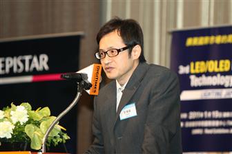
Yu-Hua Lee, R&D director of Visera
Photo: Digitimes, October 2010

