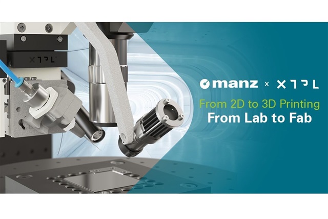
XTPL (WSE:XTP), a developer of Ultra-Precise Dispensing (UPD) technology for nanomaterial deposition, has entered a strategic partnership with Manz Asia to support the development and commercialization of advanced semiconductor packaging applications
Tracking devices play a critical role in the Internet of Things (IoT) by enabling real-time monitoring and data collection across various industries. As IoT applications expand, the demand for energy-efficient solutions becomes increasingly important. This article explores the rise of battery-efficient tracking devices and their transformative impact on IoT ecosystems.Advancements in Tracking DevicesTracking devices first emerged with the advent of GPS technology, revolutionizing location-based services. Early applications were limited, but as the Internet of Things (IoT) grew, tracking devices expanded into sectors like logistics, agriculture, and personal safety, offering real-time monitoring.However, traditional devices faced challenges like short battery life and high maintenance costs. To address these issues, advancements in energy-efficient technologies, such as low-power wireless communication and optimized sensors, led to the development of battery-efficient models. These innovations have paved the way for longer-lasting and cost-effective tracking devices that are essential for the expanding IoT landscape.How Battery-Efficient Technology WorksBattery-efficient tracking devices use low-power wireless technologies like LoRaWAN, NB-IoT, and Bluetooth Low Energy (BLE) to enable long-range communication with minimal power consumption. Sleep modes, energy harvesting techniques (such as solar or kinetic energy), and ultra-low-power processors help extend battery life.Advances in sensor technology allow these devices to collect accurate data while consuming less energy. For example, a GPS trailer tracking uses these technologies to provide long-lasting performance to ensure reliable location tracking without frequent recharging. This makes it ideal for industries like logistics that require continuous monitoring with energy-efficient solutions.Impact on IndustriesBattery-efficient tracking devices have a significant impact across various industries:In logistics and fleet management, they reduce maintenance costs and extend tracking durations for vehicles.In agriculture, smart farming solutions leverage these devices to monitor livestock and machinery with minimal energy consumption.Personal safety benefits from wearable devices that track health and location, requiring less frequent charging.Additionally, the environmental impact of these devices is profound, as longer-lasting batteries help reduce waste and the environmental concerns associated with battery disposal.Benefits Over Traditional Tracking DevicesBattery-efficient tracking devices offer several key advantages over traditional models. Longer operational life is a major benefit, as these devices can run for months or even years on a single charge, reducing the need for frequent recharging or battery replacements. This is especially valuable in remote or hard-to-reach locations.Additionally, reduced maintenance requirements lower operational disruptions, as there’s less need for battery changes or regular maintenance. Lower operational costs are another advantage, with businesses saving on battery replacements and charging infrastructure.Lastly, increased accessibility and scalability enable businesses to deploy more devices across large-scale operations, such as fleet management or asset tracking, without incurring high costs. These benefits make battery-efficient tracking devices an essential solution for industries looking to optimize their IoT networks and reduce long-term costs while enhancing operational efficiency.EndnoteBattery-efficient tracking devices are playing an important role in making IoT systems more sustainable and practical. As technology continues to improve, these devices will become even more integrated into various industries, helping to streamline operations and reduce energy consumption. The ongoing development in this area promises a future where tracking solutions are efficient and cost-effective.
Amidst the reality of global oil prices continuously skyrocketing due to war, the global market is facing the formidable challenges posed by the turbulence impacting the global economy in 2026. Major Taiwanese electronics manufacturers and supply chains are pivoting to review comprehensive AI strategies. They are adopting a particularly aggressive stance in their strategic deployment of cloud server systems and AI infrastructure, aiming to achieve an operational breakthrough where the market outlook remains far from optimistic.ASUS unveils its complete Professional Services for Sovereign AI. Since the first project in 2018, which resulted in Taiwan's first AI supercomputer, Taiwania 2, ASUS has been actively developing sovereign AI infrastructure and providing customized AI solutions to clients. Delivering trusted AI with total flexibility, from rack-scale AI Factories, desktop AI supercomputing, Edge AI to Enterprise AI solutions deployment, the company is redefining Sovereign AI Solutions with reinforces the company's position as a global leader in AI-driven digital transformation.On April 1, 2026, ASUS joins the DIGITIMES online seminar titled "Leading the Way in Sovereign AI: A Look at Next-Generation AI Computing and Storage Architecture from Supercomputing Performance". This event starts with the construction and practical application of next-generation supercomputers at the National Center for High-Performance Computing (NCHC) of the National Applied Research Laboratories. This collaborative project shows ASUS Powering NCHC to building Taiwan's AI Supercomputer and the next generation of High Performance Computing (HPC) systems.As AI and high HPC workloads push compute density and power consumption beyond the capabilities of traditional air cooling, the flagship ASUS offerings are the ASUS AI POD systems redefining the new architecture of rack-scale powerhouse, storage architecture, and liquid cooling designed for massive AI workloads. This momentum will continue to maximize computing power density through the NVIDIA HGXTM and Blackwell platforms and provide insights into solving heat dissipation bottlenecks with advanced liquid cooling technology to meet the performance and energy efficiency requirements of high-computing environments.Practical experience in building a leading infrastructure in Taiwan High Performance ComputingThe first session features a keynote lecture by Nobel Hsia, ASUS Deputy Manager of Product Planning, titled "Leading the Sovereign AI Wave: From the National Center for High-performance Computing (NCHC) projects to ASUS's Forward-Looking Infrastructure and Storage Solutions." ASUS's Sovereign AI targets the business opportunities that countries are currently striving to play the vital role of innovation in securing data sovereignty and security with in-house data processing and computing capabilities, and promotes the transformation of scientific research in the industry. ASUS has partnered with NVIDIA to build a massive AI supercomputer system with an "ALL IN on AI" strategy. Through the maximum computing power density provided by the NVIDIA HGXTM and Blackwell platforms, ASUS has deployed complete portfolio ranging from rack-scale AI factories to edge and enterprise deployment. With its proven track record of successfully supplying AI infrastructure at the B300 and GB300 levels in the market, ASUS has become a trusted partner, providing complete end-to-end solutions.It is worth mentioning that ASUS has ten years of experience collaborating with the National Center for High-performance Computing on supercomputer projects. ASUS's sovereign AI expertise is proven by several successful national-level AI project deployments, including flagship supercomputing initiatives such as Taiwania 2 and Forerunner 1, cementing its leadership in high-performance computing and AI systems. Through ASUS Professional Services, the collaboration covers all aspects from design, deployment to operation.The latest Nano4 (Crystal 26) NVIDIA HGXTM H200 cluster AI server system was to build a next-generation AI supercomputer capable of handling complex large language models (LLMs), deep learning, and advanced HPC workloads. In this new project ASUS has built Taiwan's first AI supercomputer project based on NVIDIA GB200 NVL72 system architecture with direct-cooling technology. The engineering team has played an important role in the delivery of the servers, the planning of large-scale computing architecture, deployment and optimization, which has become the foundation for ASUS to expand its overseas AI deployment and demonstrate ASUS's ability to build computing power from national to international levels.Opening Agentic AI Frontier: ASUS Supports NVIDIA Vera Rubin Platform and InfrastructureIn response to the advent of the new-generation NVIDIA Vera Rubin platform and its accompanying infrastructure architecture, ASUS has developed the next-generation ASUS AI POD highlighting a proficiency in liquid-cooled AI solution. Spanning the new design from rack-scale AI factories, data center servers to desktop workstations and edge AI devices, this solution delivers end-to-end AI computing power and infrastructure, specifically targeting trillion-parameter models and million-token contexts, maximizing efficiency across power, memory, and compute.Hsia began by introducing the ASUS flagship XA VR721-E3 architecture. This system supports the NVIDIA Vera Rubin NVL72 platforms; it is purpose-built for large-scale AI model inference and training to deliver massive AI performance for large-scale AI factories. while also accommodating the specific workloads required for agentic AI. Designed as a 100% liquid-cooled, rack-scale system, it features a Thermal Design Power (TDP) reaching up to 227 kW, which is a capability that fully satisfies the demand for the immense performance required to compute AI models with trillions of parameters.Furthermore, addressing rigorous enterprise-grade data-center demands, ASUS has simultaneously launched the XA NR series. These product series support the NVIDIA HGXTM Rubin NVL8 architecture, featuring eight Rubin GPUs interconnected via the sixth-generation NVLink, which each GPU could deliver a maximum bandwidth of 800 GB/s. To facilitate a seamless and cost-effective transition to liquid cooling, ASUS offers two distinct solutions: the XA NR1I-E12L, an innovative hybrid-cooled option; and the XA NR1I-E12LR, a 100% liquid-cooled system.To support these powerful systems and democratize AI development, ASUS also has established a robust data ecosystem by partnering with NVIDIA-Certified storage providers. The storage solutions offers the technologies such as JBOD, DPDK, and Object Storage, thereby delivering scalable, resilient solutions for memory-intensive AI applications to support robust capabilities for the integrated storage and operational management.On the software front, ASUS provides a suite of one-stop platforms. Leveraging the ASUS Infrastructure Deployment Center (AIDC), ASUS automated the setup process including ACC (ASUS Control Center) and BMC, accelerating time-to-market for critical research resources. To address the full spectrum of requirements for system construction, deployment, and operations, ASUS provides expert consultation, a broad portfolio of tailor-made AI solution while simultaneously catering to the comprehensive lifecycle management needs of the entire data center.WEKA data storage platform is redefining AI storage economicsTo meet the elastic data storage requirements of AI workloads across diverse usage scenarios, ASUS's AI POD system incorporates a comprehensive storage solution featuring a high-speed, All-Flash NVMe SSD storage architecture. ASUS has collaborated with its ecosystem partners to develop a next-generation unified storage system with high-reliability storage servers and professional validation of network. WEKA, the AI storage company, is one of partners providing high-performance, software-defined storage for GPU-accelerated AI and HPC environments, combining low latency with unified data management.In the second presentation of the session is delivered by Ray Wu, Senior Consultant for the Asia-Pacific region at WEKA. His speech titled the theme "Ultimate Data Empowerment: How WEKA Helps NCHC Build an AI-Accelerated Computing Storage Architecture". To address NCHC's requirements for extreme performance and energy efficiency, Wu highlighted the unified data management solutions to provide rapid scalability, which emphasizing flexibility and intelligent adaptive capabilities, and effectively addressing the demands of a wide array of usage scenarios.Addressing the requirements of diverse application environments such as Kubernetes and Slurm in NCHC Nano4, WEKA serves as the high-performance storage foundation through its efficient storage platform. Based on the NVIDIA AI Data Platform reference architecture, the solution employs an end-to-end system to accelerate data processing performance for HPC applications. This assists the NCHC in optimizing the deployment of high-efficiency AI computing, dramatically reducing the time required for AI application deployment and development from months to mere minutes.This ASUS WEKA storage solutions demonstrates the NCHC's technical excellence in leveraging its ecosystem and integrated services to rapidly deliver the low-latency, scalable and high throughput required capabilities and swiftly support the next generation of agent-based AI applications. WEKA solutions empower enterprises to transition from experimentation to full-scale operations, rendering AI applications economically viable and maximizing performance across a wide spectrum of fields, ranging from next-generation AI agent systems to AI-enabled healthcare applications.In this event, ASUS showcases fully liquid-cooled AI infrastructure with the critical thermal management required for the next-generation NVIDIA Vera Rubin NVL72 system platform. By efficiently dissipating heat from high-performance CPUs, GPUs, and accelerator-dense racks, ASUS significantly reduces energy consumption while supporting unprecedented rack density to enable enterprises and cloud service providers to build high-performance, energy-efficient large-scale AI clusters with unmatched efficiency and dramatically reduced PUE and TCO.【White paper download】Empowering Scalable AI Reasoning with ASUS AI POD featuring【Webinar on-demand】Bridging NCHC Success to NVIDIA Vera Rubin Architecture
HQ Pack is a global leader in high-tech packaging solutions. The company is expert at designing, producing, (precision) cleaning, and making packaging solutions reusable again after use, as well as manage the packaging logistics of high-quality industrial products. They do so for clients in the semiconductor and other high-tech industries. The process procedures and packaging solutions ensure the parts, modules or components of highly sophisticated equipment are fully protected during transportation and logistical arrangements. And at the same time, the system will meet the customer demand for protection of valuable products during transit while adhering to environmental, social, and governance (ESG) principles. The packaging design incorporates features like sustainable materials, waste reduction strategies, and carbon footprint minimization, alongside ensuring the integrity of high-value goods through robust physical protection. The company provides complete packaging solutions, starting with the development and sourcing of customized packaging materials. HQ Pack's regional Service Centers ensure that reusable packaging materials are ready to use again by cleaning and repairing them to like-new condition. They can also support reuse of parts by harvesting them before scrapping for new build packaging. If there is material destined for waste management, HQ Pack supports this at the same time.Because most of its high-tech clients operate on a global scale, HQ Pack operates not only at its headquarters in Eindhoven, the Netherlands, but also in Johor and Penang in Malaysia, Taiwan, Singapore, Germany, and in the United States (locations in Brookfield (CT), Newark (CA), and San Diego (CA)) providing the same quality and service at each location. With their Service Centers they support both their customers' sustainability goals as well as their own. Their slogan "We Create to Protect" is exactly what they do. The high-quality packaging solutions ensure that valuable and fragile products, modules, components and/or parts can be safely transported worldwide. With over 40 years of experience and global presence, no compromission on quality, flexibility at the heart of our organization, they are a full-service provider with fast, reliable and sustainable packaging solutions.
DigiKey, has introduced an industry-power supply configuration tool, which simplifies the process of designing power supply solutions.Developed for engineers, designers, and system integrators, this intuitive online tool enables the quick selection of key attributes - such as outputs, voltage, current and more - to generate a tailored power supply solution that meets users’ desired requirements. Once configured, the custom power supply is assembled and shipped directly within days. Hosted on DigiKey's trusted, high-performance website, the configurator enables fast and accurate selection and sourcing - making it easier than ever to design, customize and order the right power solution for the project."DigiKey is thrilled to offer this industry-first tool that allows our customers to configure their own power supply independently," said Heather Fulara, senior director, interconnect and electromechanical for DigiKey. It dramatically reduces the time it takes to acquire a configured unit, which allows for more efficient workflows, saving time and accelerating design.The tool available from DigiKey currently features the NEVO+ and VCCM series from Vox Power, which is the first supplier involved in the program."Vox Power is proud to collaborate with DigiKey as the first supplier to participate in this innovative, time-saving tool," said Marco Prinsloo, co-owner of Vox Power. "We trust DigiKey's expertise in making our customers' designs come together seamlessly through its efficient online design and customization options."
The European Union Artificial Intelligence Act (EU AI Act) is set to be fully implemented in 2026, and the Cyber ??Resilience Act (CRA) is scheduled for 2027. Adding the Radio Equipment Directive Delegated Act (RED-DA) already took effect on August 1, 2025, those three legislative measures collectively emphasize mandatory requirements for information security and cybersecurity.These regulations strengthen the comprehensive lifecycle management mechanisms for critical applications, IT components and telecommunications, impacting corporate strategies for complying with international information security standards while providing new opportunities for next-generation technological innovation. As a globally leading standards testing and certification organization, TUV NORD combines multiple international standards to meet comprehensive regulatory requirements, helping global enterprises address major challenges in AI, cybersecurity, and information security regulations.Eric Behrendt, Global Key Account Manager of TUV Information stechnik GmbH (TUVIT), and Chia-Hung Lin, Director of the Information Security Business Division at TUV NORD Taiwan, were jointly interviewed. This interview coincided with the relocation of TUV NORD Taiwan's testing laboratory to its new address in Kaohsiung City. Taking advantage of the new facility's inauguration. In addition to inviting industry customers to celebrate together, they introduced TUVIT's global organizational developments and its comprehensive assessment and verification services, helping Taiwan customers understand new information security standards and the laboratory's development to seize new market opportunities.TUVIT is an independent subsidiary within the TUV NORD Group, dedicated to the Digital and Semiconductor Business Unit, focusing on information security and data infrastructure resilience technologies. Established in 1995, TUVIT provides cybersecurity verification, testing, and consulting services, specializing in establishing information and networking security technology, testing hardware, software and certifying information security management systems. With the global industry's growing emphasis on and attention to semiconductor chips and network equipment information security standards compliance, TUVIT has established a robust information security environment to advance technological progress and ensure digital security.In partnership with TUV NORD Taiwan, TUVIT assists Asian semiconductor, electronics manufacturing, and OEM/ODM manufacturers in obtaining certifications for various international and national information security standards. This will include Germany Federal Office for Information Security (or named BSI) IT Baseline Protection to enhance cybersecurity with a structured framework for organizations to protect their IT systems effectively.TUV NORD Taiwan laboratory offers services for CC, FIPS 140, and FIDOTUV NORD Taiwan, together with TUVIT, has collaborated to help assisted 12 semiconductor customers in the Asia-Pacific region (across more than 20 factories) achieving the German BSI Common Criteria safety certification. TUV NORD Taiwan's Kaohsiung testing laboratory is the only laboratory in Taiwan equipped to certify three major international cybersecurity standards including Common Criteria (CC), the U.S. National Institute of Standards and Technology (NIST) FIPS 140-3 standard, and the Fast Identity Online (FIDO) standard.TUV NORD Taiwan has further expanded its services to include financial and industrial PC sectors, in addition to its existing work in semiconductors and networking, to help Taiwanese electronics manufacturers meet global compliance requirements. This expansion offers a broader range of services like product safety, information technology, and vendor assessment audits to support companies in navigating complex global standards.Meanwhile, TUVIT also has expanded more actively into emerging fields such as artificial intelligence and quantum computing certification services, which are key technologies poised to redefine problem-solving, innovation, and competitive landscapes. TUVIT supports companies in implementing these new requirements and contributes to the safety and reliability of emerging technologies in the post quantum era.As AI technologies become increasingly integrated into everyday business operations, ensuring ethical, transparent, and secure AI systems is very important. The AI Act is the first legal framework on AI, which addresses the risks of AI and positions Europe to play a leading role globally. Since 2018, BSI has reacted quickly to the rapid development in the field of artificial intelligence and created a framework that keeps pace with technological developments. This also includes intensive testing and the implementation of countermeasures. TUVIT carried out these tests and began developing and applying initial testing methods for AI applications at an early stage, Behrendt highlighted. He proudly stated that TUVIT continues to work closely with BSI to ensure compliant in AI devices keeping pace with rapid technological advancements.NIST Post-Quantum Cryptography Standards become a key role in Information security certificationUsing Quantum Key Distribution (QKD) technology as an example, Behrendt noted that the threat of quantum computer attacks on classical cryptographic mechanisms must be considered to ensure future-proof protection of information. QKD offers a promising solution by harnessing the principles of quantum mechanics to establish secure keys. TUVIT assists enterprises in following NIST-adopted Post-Quantum Cryptography (PQC) standards, providing industry testing and certification services to ensure their systems can withstand future quantum computer attacks.Of course, this also involves enterprises' information systems requiring continuous assessment and upgrades to adapt to the practical operational needs of new PQC algorithms. Current cutting-edge technological developments involving data transmission and remote data exchange all require secure certification mechanisms for assurance. TUVIT is working with global technical partners to develop testing technologies and equipment, enabling related certification work and standard development to proceed in parallel.Beyond facing new challenges such as QKD technology, customers currently face multiple certification requirements including CRA and EU AI Act standards, which inevitably leaves them feeling overwhelmed. Behrendt recently participates in three or more technical consultation meetings with customers regarding CRA standards almost every week. He observes that many customers neglect preparations from the initial stages of product design planning. He especially reminds customers of the importance of a secure internal product development framework that considers information security planning.Large or middle scale manufacturers meet multiple product line launch requirements by leveraging a common product development or manufacturing platforms that incorporates information security standards from the start. This enhances the security of specific environments and allows for the reuse of verification results when certifying products manufactured in those environments, thereby simplifying subsequent product certification processes, saving time and costs.Furthermore, regarding CRA and AI Act, he provides several strategic recommendations. First, priority attention should be given to CC for IT security evaluation and IEC 62443 for industrial automation system information security standards. Currently, these fundamental cybersecurity standards have become prerequisites for new products entering international markets. Furthermore, for consumer electronics product cybersecurity requirements, all security requirement items will require to follow ETSI/EN 303 645 IoT network security standards as important cybersecurity requirement guidelines.Since Taiwan's electronics industry consists major OEM/ODM manufacturers for global brands, TUV NORD Taiwan supports Taiwan's electronics supply chain by providing premium testing, inspection, certification, and consulting services to meet the specifications requested by global branding customers. These services help ensure that products comply with safety , quality, and cybersecurity standards across various industries, and contribute to market access and customer confidence.Behrendt sincerely advises Taiwan OEM/ODM customers that from the first day of designing products under CRA, they must consider security and information security design. If these requirements are not considered, ultimately they will still need to go back to resolve these compliance challenges. Once these basic requirements are overlooked, regulatory agencies for these new standards will impose high penalty as punishment, which will cause product brand name value and enterprises to suffer significant losses. Therefore, he recommends that enterprises need to take seriously and genuinely prepare response plans early and avoid violations. Passing certification and presenting evidence of proven effectiveness is the best product compliance strategy.FIPS 140-3 Cryptographic Module and Software Testing Compliance GuidelinesGovernment agencies in the United States and Canada require FIPS 140-series certification for cryptographic products, while Taiwan's requirements align with this international standard. This certification is mandatory for products used to protect sensitive information and ensures that cryptographic modules have been independently tested and validated for security.Since cryptographic applications involving information exchange and sharing are not limited to hardware or software, as long as they participate in encryption and decryption operations, they need to pass FIPS 140-3 certification. For example, the systems including operating system software, semiconductor chips, network routers, firewalls, and other hardware devices all require to grant the requiring certification.TUV NORD Taiwan's cryptographic module testing laboratory in Kaohsiung is the only local laboratory specifically providing testing and consulting services for this standard. Teddy Tsui, Senior Manager and FIPS 140 Lab Director, introduced that TUV NORD Taiwan laboratory obtained FIPS laboratory certification in 2014. This laboratory is also the only one in Taiwan recognized by NIST, serving ASIA customers for over ten years with expertise in the cybersecurity field. Currently, the laboratory can perform FIPS 140-3 testing for three types of cryptographic validation including hardware cryptographic modules, software algorithms, and entropy sources. Meanwhile, this lab also provides customer consulting and educational training.Credit: TUV NORDTsui explained that the Cryptographic and Security Testing (CST) laboratory only conducts testing and issues test reports for a FIPS 140 standard certification. But the NIST is the authority that issues the formal certification or validation. Talking about the time consuming for hardware cryptographic modules, the process will include checking design process documentation, functional testing, and even code inspection are required.The average time for a FIPS 140-3 certification for hardware cryptographic modules is approximately from 18-month to 2-year, largely due to a backlog caused by the transition from FIPS 140-3 and the high volume of requests, which contributes to the extended waiting period. But software algorithm testing is relatively faster. The laboratory uses software verification programs, expecting to complete testing in two to three weeks. Since NIST released three PQC standards for algorithms that can resist quantum computer attacks in August 2024: FIPS 203 (for key encapsulation), FIPS 204 (for digital signatures), and FIPS 205 (for hash-based digital signatures). These algorithms are now available for certification testing.NIST estimates that quantum computers could threaten current cryptography in the next 10 years, leading to risks for long-term sensitive data through the "harvest now, decrypt later" attack. This involves attackers collecting encrypted data today and decrypting it in the future when a powerful enough quantum computer becomes available.Tsui also frankly stated, FIPS 140 standards for software algorithm testing will require re-testing when PQC algorithms are updated. Customers will face challenges in migrating their systems. The main challenges include the complexity of inventorying all cryptographic systems, integrating the new algorithms into products, and the long timeline for the transition, which requires careful management and strategic planning.TUV NORD Taiwan Leverages Localization Advantages with Rich Experience Serving Taiwanese ManufacturersFurthermore, Chia-Hung Lin, Director of the Information Security Business Division at TUV NORD Taiwan, especially emphasized the importance of information products passing CC verification. The requirement starts from the entire product development lifecycle to ensure cybersecurity every stage of the manufacturing process receives complete protection.The evaluation process of CC certification will include Site Certification where product development or manufacturing occurs. This is ensuring that the physical and procedural environment where a product is developed or manufactured meets security standards, protecting design data and products throughout their lifecycle. These audits are crucial steps in the evaluation, as it validates the developer's claims about product security and confirms the integrity of the entire supply chain, not just the final product itself. Meanwhile, Site Certification also saves time and money for re-audits by allowing a single certification to cover multiple products developed or manufactured at that site. Currently, the major semiconductor fabs and OSAT vendors in Taiwan have obtained Site Certification with TUV NORD Taiwan's assistance.Among the experience of serving Taiwanese customers for decades, most notably, Lin pointed out one real case for customer support in Taiwan. The COVID-19 pandemic induced systemic disruptions by semiconductor shortage for the auto industry during the years in 2020. At that time, Taiwan government has implemented strict border quarantine for all passengers. A Taiwanese semiconductor fab manufacturing automotive chips urgently needed certification but caused delays for the quarantine policy with TUVIT German auditors and professionals. TUV NORD Taiwan's team overcame difficulties and communicated with the government, resulting in a breakthrough that allowed German auditors perform audits on time to certify this Taiwanese customer. This case becomes an important case in TUV NORD Taiwan's customer support history.TUV NORD Taiwan maintains an important market reputation and actively maintains long-term relationships with customers. Combined with the unique and important value demonstrated by the localized laboratory - not just testing equipment, but also the extensive practical experience and know-how accumulated over the years - TUV NORD Taiwan's services have earned customer trust. With Global information security product opportunities to increase Asian manufacturing by helping companies diversify supply chains, TUV NORD Taiwan aims to partner with Taiwan clients to leverage new business opportunities that arise from information security standards. This partnership focuses on helping customers to seize the critical business opportunities on the growing importance of cybersecurity by ensuring compliance with standards, protecting sensitive data, and maintaining business resilience.Credit: TUV NORD
HITEC Power Protection develops, manufactures, and provides dynamic uninterruptible power (UPS) solutions to support the most vital of manufacturing and business critical applications. Founded in 1956, its products are widely used in industries with high power reliability requirements, such as semiconductor fabs, banking, aviation, healthcare, and government defense, to ensure that critical missions and processes receive uninterrupted and stable power supply. HITEC Power Protection provides equipment to ensure safe, reliable, and adjustable power to support the operational needs of businesses and critical government facilities. Taking ESG and sustainability into consideration, HITEC Power Protection provides customers with solutions to meet the demanding and complex operational needs of the high-tech industries by providing immediate, reliable backup power and voltage regulation during outages.The company has accumulated over 60 years of experience in industries requiring high power stability, primarily using flywheel energy storage technology. This technology stores energy in a mechanical flywheel to ensure immediate emergency response and stable power supply in the event of power anomalies. Once an emergency power outage is detected, the flywheel energy storage system will be activated to deliver stored instantly, and within 5 seconds transfers smoothly to an integrated diesel generator to provide long term emergency power. HITEC Power Protection was introduced to the Taiwanese market in 1985 and has successfully installed over 200 units. Its customers primarily include well-known semiconductor manufacturing fabs and the display panel makers. As Taiwan's industrial demand for power stability continues to rise, the business opportunities of HITEC Power Protection continue to grow.The current product line provides a continuous power generation capacity of approximately 2,880 kW at 60 Hz per unit. And the features include power safety and protection functions, such harmonic filtration, surge protection, load stabilization, and short-circuit current protection, which outperform typical static UPS systems. HITEC Power Protection provides 100% emergency power to all manufacturing and supporting equipment, implementing precise UPS capacity design to ensure a stable power supply to customer's power loads. This not only reduces unstable power risks but also overall lowers installation and ongoing maintenance costs. After engaging the market with Taiwanese industrial clients, HITEC Power Protection is now further targeting the needs of reliable backup power systems for major government critical public facilities, such as disaster prevention and instant response systems for critical infrastructure like tunnels and airports, with the ultimate goals of improving public service quality, bolstering private sector disaster preparedness, and significantly enhancing the overall resilience of Taiwanese society.
Founded in 2020, Powertrim Technologies is a provider of back-end packaging equipment for power modules. Rooted in over 40 years of semiconductor trim and form toolmaking heritage, the company offers product design support, prototyping, and manufacturing services for power modules used in electric vehicles, the energy industry, and industrial applications. The rapidly growing automotive industry is driving significant demand for compound semiconductors and back-end packaging to support the growth of power modules, creating a strong demand for power module packaging and manufacturing technologies. The company offers full support to allow power module manufacturers to predictably build quality products at the most competitive price.The Powertrim Flex Line, the flagship manufacturing platform, provides high performance handling, assembly and testing technology for automated power module manufacturing. With its modular architecture, the Flex Line covers the core trim and form processes as well as adjacent process steps like laser marking, laser de-flashing, optical inspection, quality control, testing, loading and unloading.The main focus of Powertrim Technologies is in providing power module back-end packaging equipment and tooling. Through different modular machine designs, they are assembled into production configurations that meet the customized needs of various power module products. The company also provides the well-designed tools to help customers implementing both prototyping, qualification and rapid serial or mass production of power modules.Furthermore, electrification of the automotive transmission system by either battery or hybrid electric motors, new industrial power applications and the massive growth of renewable energy solutions accelerate the need for power modules. With these, Powertrim provides manufacturing equipment, supporting a wide range of power electronics applications, and is strategically collaborating with supply chain partners to centralize services and resources for the EV market, a move designed to meet fluctuating demands efficiently.The existing flagship production line implements a system designed to adapt quickly to changes in product type and quantity, allowing for the efficient production of a variety of power module products on one single machine, hence Flex Line. With this concept, the company is capable of switching between complex product sizes in under 15 minutes. In addition, it can also provide a series of optional add-on units, including loading/offloading modules, laser marking & de-flashing, automatic optical inspection, MES integrated system, which providing software linking to ERP/MES enterprise software platforms. These different arrangements can be flexibly matched and assembled to meet the manufacturing needs.With a presence in the Netherlands, known for its cutting edge semiconductor front-end and back-end equipment, Powertrim Technologies combines precision engineering with scalable automation to unlock markets such as automotive, energy and industrial power applications. At Semicon Taiwan 2025, Powertrim aims to work together with Taiwanese customers to create new opportunities.
Tempress is a leading manufacturer of diffusion and thin film deposition equipment, with over 55 years of experience in thermal process technology. We support innovators in semiconductors, power, MEMS, photonics, memory, life sciences, and coating industries in producing high-value materials and devices. Our production systems are built for R&D applications but also for automated, high-volume production and meet the rigorous standards of modern chip manufacturing. Tempress solutions cover essential thermal processes such as oxidation, annealing, diffusion, and LPCVD, offering precise temperature control to achieve optimal properties in silicon wafers.Tempress established an early presence in Taiwan (1999), earning recognition across the region's semiconductor sector. Our local experts ensure smooth coordination between customers and our product team in the Netherlands, providing hands-on support and technical guidance.We collaborate globally with universities and research institutes to drive innovation and continuously improve our technology. At Tempress, we deliver more than equipment-we build lasting partnerships backed by dependable service and worldwide support.
Trymax Semiconductor B.V. provides plasma-based etching, stripping, and curing process equipment for advanced semiconductor packaging, targeting applications in dry descum, ashing, surface preparation, light etching and processing, as well as UV photoresist curing and charge erase. It also manufactures UV curing equipment, focusing on equipment used in compound semiconductor processes. These equipment are used in the production of wide-bandgap semiconductor power devices such as silicon carbide (SiC) and gallium nitride (GaN), as well as other important processes such as communication power amplifiers (PAs).Trymax has been established for over 25 years and has a considerable customer base and brand recognition in the Taiwanese market. At Semicon Taiwan 2025, the company primarily serves to promote its products and connect with key clients. With a product portfolio ranging from 100mm to 300mm wafer size, Trymax's clients are on both sides of the Taiwan Strait becoming major suppliers to the manufacturers of power amplifiers and RF components. In the global presence, Trymax has significant market shares at foundries, IDMs and wafer level packaging houses for end applications in Power semiconductor, automotive, MEMS, LED and CMOS.Trymax's NEO series plasma dry descum systems are suitable for cleaning and activation processes in the semiconductor industry, offering high efficiency, uniformity, and repeatability. These systems utilize RF/microwave power to generate high-energy, disordered plasma under vacuum conditions. They can process a wide range of substrate sizes and offer a variety of processing technologies for flexible customer selection, meeting the needs of diverse semiconductor process technologies.Trymax continuously innovates to support its customers’ needs. In addition to the compound semiconductor processes, it is also widely used in application fields such as MEMS microelectromechanical systems, microfluidic devices, SOI substrate manufacturing, advanced packaging and optoelectronic displays. Among them, the global installed capacity of NEO system equipment has exceeded 300 sets.
Invest in Holland /Netherlands Foreign Investment Agency (NFIA) is the national investment promotion service of the Netherlands. It operates as part of the Dutch Ministry of Economic Affairs, supporting foreign companies in establishing and expanding their businesses in the Netherlands. The organization works with a network of regional partners and has a global presence through its worldwide network of offices, including one in Taipei, to facilitate foreign investment and economic development. With 25 offices worldwide, Invest in Holland has over 40 years of service experience. The Taipei office assists Taiwanese companies in developing their businesses and R&D IN EUROPE and expanding the opportunities in the Netherlands. The services include to provide customized information on the Netherlands, relevant business locations, Dutch legislation and tax regulations, labor law, permit procedures, government incentives and much more through in-person or digital meetings. With a population of over 18 million people, the Netherlands economy relies on international trade. It is highlighting the importance of foreign investment to strengthen its innovation ecosystems and achieve future economic goals. The network of Invest in Holland actively promotes this idea by focusing on sectors like high-tech industries, and sustainable energy, where collaborations between companies, government, and knowledge institutions drive innovation and economic resilience. Right now, more than 230 Taiwanese companies have setup their European headquarter or R&D center in the Netherlands. Many of which companies are in the Semiconductor and ICT-related sector, eg CHROMA, DELTA ELECTRONICS, MIC, ADVANTECH, and etc.Invest in Holland actively creates opportunities for industrial clusters to develop in the Dutch market by attracting Taiwanese companies and fostering collaboration between businesses, high-tech research institutions, and government, enabling Taiwanese companies to quickly integrate into the local operation and accelerate business development. One important thing, Invest in Holland's services are entirely free for all foreign companies, both new and established, that are looking to expand their operations into the Netherlands. This is a benefit provided by the Netherlands government and its network of partners. These public services offer guidance, practical solutions for establishment, and connections to the right resources and partners to help international businesses succeed in the European market.