![]()
Tuesday 26 May 2026
ONEKEY Partners with Trinity Technologies to Conquer CRA Compliance
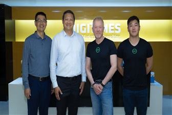
With the first phase of the European Union's Cyber Resilience Act (CRA) set to take effect imminently, German-based automated cybersecurity compliance provider ONEKEY, together with its Taiwanese local partner Trinity Technologies, notes that the CRA elevates product cybersecurity from a "one-time audit" to a "long-term governance" framework. Its review documentation and reporting processes are subject to an extremely rigorous compliance framework. To this end, ONEKEY and Trinity Technologies jointly recommend that Taiwanese ICT companies prepare early, leveraging localized professional support and automation tools to complete verification, and transform compliance pressures into market competitiveness.Cybersecurity Management Obligations Extend from Shipment to the Entire Lifecycle, Making Reporting Mechanisms a New Challenge for EnterprisesThe CRA will first implement vulnerability reporting and response mechanisms on September 11, 2026, and will take full effect on December 11, 2027. At that time, companies that have not achieved compliance will not only face substantial fines but may also see their products banned from sale in European countries. The CRA requires that all "Products with Digital Elements" (PwDE) fully incorporate cybersecurity management during planning, design, development, and maintenance, and address vulnerabilities throughout the entire product lifecycle. Consequently, most information and communications technology (ICT) supply chains—including smart home devices, connected devices, industrial control products, automotive electronics, and software solutions—are directly facing the impact of CRA regulations.Although the CRA is set to take effect in early September, a survey by ONEKEY reveals that as many as 68% of companies remain unfamiliar with the specific details of the CRA. ONEKEY notes that most manufacturers face four common misconceptions regarding the CRA regulations. First is a misjudgment of the implementation timeline, overlooking the fact that the "24-hour vulnerability reporting obligation" will take effect on September 11, 2026;second is a misunderstanding of responsibility, failing to elevate product safety to the level of "product governance"; third is a lack of compliance evidence, as a single penetration test is no longer sufficient to meet EU audits; and finally, manufacturers must be responsible for the overall safety of their products, which means the entire product supply chain must also comply with the CRA regulations.Five-Step Guide for Manufacturers to Build a Reproducible Operational Model, Starting with a Product Line InventoryJan Wendenburg, CEO of ONEKEY, stated: "We are at a turning point where global products face stringent cybersecurity requirements. With the EU's implementation of the CRA, cybersecurity is no longer a 'nice-to-have' for products, but rather a 'passport' for entering the European market. Many manufacturers possess world-class hardware engineering capabilities, but when faced with complex software supply chains, they often lack real-time, auditable transparency. ONEKEY's mission is to help clients bridge compliance gaps, guiding them from a 'good enough' approach toward full lifecycle cybersecurity governance."To transform this situation, ONEKEY leverages integrated platform technology to weave SBOM automation, vulnerability prioritization, impact assessment, and compliance guidance throughout the entire product lifecycle. This helps manufacturers establish a monitoring system ready for audits at any time, fundamentally resolving compliance challenges. Currently, ONEKEY has assisted global giants in Taiwan—including and ZyXEL—in aligning with CRA compliance requirements. Leveraging its extensive experience in CRA compliance, ONEKEY recommends that manufacturers follow these five steps to progressively achieve CRA compliance, thereby creating a repeatable compliance operating model. This transforms product "compliance" into a powerful competitive advantage, enabling them to seize the initiative in the European market. 1. Assess the product portfolio: Prioritize identifying which networking equipment, industrial computers, or IoT devices will be sold in the European market after 2026 and 2027. 2. Comprehensively establish a Software Bill of Materials (SBOM): For the aforementioned products, create an SBOM by scanning source code and binary code, ensuring it includes legacy firmware and vendor-provided firmware.3. Establish a Product Security Incident Response Team (PSIRT) process: Ensure that a dedicated team can assess the scope of impact within 24 hours of a vulnerability disclosure, fulfill reporting obligations, and proactively implement remediation.4. Implement "Shift-Left" Development: Integrate binary analysis and SBOM checks into every software development and firmware release cycle as a final pre-shipment verification.5. Turn Evidence into a Marketing Asset: Encourage the public disclosure of these automated detection results and compliance evidence to demonstrate product security as a key differentiator to European buyers.Incorporating AI Compliance Pathways Aiming for 100% Certainty into Automated TestingRegarding the application of AI in automated testing technology, ONEKEY emphasizes that while AI adoption certainly improves efficiency, it must also adhere to non-negotiable standards of determinism for cybersecurity compliance. Unlike the generative AI commonly found in the market today—which is prone to "hallucinations" or misjudgments—the AI models adopted by ONEKEY focus on the auditability and accuracy of results. Wendenburg stated, "In the realm of legal compliance, 'mostly correct' is 'wrong.' When EU auditors request proof of compliance, vendors cannot provide a result that is merely a guess generated by AI."To implement "Responsible AI," ONEKEY's technical architecture combines in-depth binary static analysis with rigorously validated deterministic algorithms. This means that every decision made by the system—whether scanning firmware, generating an SBOM, or matching against CRA regulatory requirements—is backed by clear logical reasoning and technical evidence. This approach ensures the system does not produce false regulatory determinations, preventing enterprises from falling into compliance traps due to AI false positives and even facing unnecessary legal litigation risks.Wendenburg emphasized that cybersecurity compliance requires not an AI that writes poetry, but a digital audit assistant with a high degree of "certainty." Through this rigorous technical approach, ONEKKEY assists Taiwanese companies in navigating the complex provisions of the CRA to produce legally valid compliance evidence that withstands official EU verification, reducing the error rate in regulatory judgments to near zero and fundamentally protecting the company's market reputation and operational rights.Trinity Technologies Strengthens Localized Technical Support to Help Manufacturers Become Trusted Security Partners in the EUChen Zhaoren, founder of ONEKEY's Taiwanese partner Trinity Technologies, pointed out that as a global hub for the ICT industry , time has become the most pressing cost factor for enterprises in Taiwan as the EU's CRA regulations are set to take effect. He observed that while Taiwanese contract manufacturers have traditionally relied on "fast delivery" and "value for money" as their core competitive advantages, future market dynamics will shift toward "Secure by Design" and "supply chain transparency." Currently, EU brands have begun formally shifting the responsibility for providing Software Bill of Materials (SBOM), vulnerability reporting obligations, and up to five years of security maintenance to their Taiwanese supply chain partners. This means that Taiwanese manufacturers can no longer remain on the sidelines of this compliance wave.To help enterprises navigate these stringent regulatory hurdles, Trinity Technologies is committed to localizing world-class tools like ONEKEY to assist Taiwanese companies in reshaping their R&D and quality assurance management processes. Through comprehensive protection technologies that integrate source code and binary firmware, Trinity Technologies helps manufacturers establish automated compliance evidence chains and vulnerability response mechanisms without sacrificing cost-effectiveness. This not only accelerates clients' procurement review processes but also helps Taiwanese manufacturers transition from mere hardware suppliers to "security strategic partners" trusted long-term by the EU market, enabling them to withstand low-cost competitors in a regulation-driven competitive environment.Smart Compliance Wizard and Fast Start Program Helping Enterprises Simplify Processes and Accurately Identify GapsTo help clients quickly grasp, organize, and implement the CRA regulations, ONEKEY has launched the "CRA Fast Start" acceleration program—specifically designed for equipment, machine, and system manufacturers—to assist companies unsure where to begin. Through automated software, the program addresses three key areas—readiness assessment, systematic vulnerability management, and 24/7 continuous monitoring—to guide companies step-by-step in identifying gaps in their existing processes and precisely pinpointing discrepancies with compliance standards.Additionally, ONEKKEY actively participates in the EU-funded Digital Europe program "CRA Compliance Wizard" and has integrated it into its products to provide automated guided workflows. Customers need only upload firmware binary files; the system automatically analyzes vulnerabilities and compares them against regulatory requirements, guiding enterprises through technical and organizational questions to generate a CRA-compliant "Statement of Compliance" and audit trail with a single click. This streamlines the previously cumbersome process of manually creating documents—which required significant legal and engineering resources—transforming it into an intelligent software tool that simplifies regulatory compliance in daily operations.If addressing EU CRA regulations is likened to a military campaign, "CRA Fast Start" serves as a "training and advisory program" that helps enterprises inventory their resources, formulate strategies, and build a defense system; meanwhile, the "Compliance Wizard" is the "intelligent detection weapon" used by R&D and QA personnel in actual operations to scan for product vulnerabilities, accurately answer regulatory questions, and generate certificates of compliance. The two complement each other, not only simplifying complex processes but also helping manufacturers transform compliance costs into a strategic advantage for entering the European market.Actively Preparing for the Phase 1 Deadline: Turning Compliance Pressure into a Strategic Advantage for Entering EuropeAs the September 11 deadline for the first phase of vulnerability reporting obligations draws near, Taiwanese ICT manufacturers can no longer afford to sit on the sidelines. The entry into force of the CRA not only signifies a comprehensive raising of the EU's product cybersecurity standards but also marks a survival-of-the-fittest test of supply chain resilience. Faced with extremely complex review documents and the stringent 24-hour reporting deadline, traditional manual response models can no longer meet compliance requirements. If manufacturers fail to promptly establish an automated vulnerability management and continuous monitoring system, they not only face the legal risk of product withdrawal from the market but may also lose their competitive edge as EU brands reshape their supply chains.Amid this tidal wave of compliance, the first step in proactive preparation lies in implementing a "product safety incident response team," "shifting security left," and "supply chain transparency." Through ONEKEY's automated compliance tools and Trinity Technologies' localized professional support, enterprises can start by inventorying their product lines to rapidly build highly reliable SBOMs and technical evidence chains. This transformation effort should not be viewed as a burdensome "compliance tax", but rather as a "market passport" for building international trust and countering low-cost competition. By taking action now and leveraging automation to bridge process gaps, companies can confidently turn regulatory challenges into a powerful moat for deepening their presence in the European market when the new regulations take effect in 2026.ONEKEY and Trinity Technologies meet to discuss CRA compliance solutions. Credit: DIGITIMESONEKEY CEO Jan Wendenburg explains CRA regulations and strategies for Taiwanese ICT companies. Credit: DIGITIMES