Amigo-LLM: AI-enabled electronic design automation for increased first-silicon success
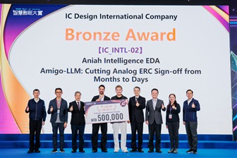
"Integrated circuit" is a fancy term for the chips that control the electronics that make our modern life possible. They are composed of hundreds of thousands or even millions of tiny components, such as transistors, capacitors, and resistors. These components are so tightly linked together on a tiny piece of silicon that, for all intents and purposes, the chip is indivisible – you can't separate it into its individual components.Any mistake in a chip's circuitry could thus render the entire chip unusable. The process of transferring the as-yet theoretical chip design to the fabrication plant (also known as a foundry or chip fab) to produce a photomask (the template that will later be used to create chips en masse) is known as the tape-out, and costs in the tens of millions of dollars.So chip designers have a strong financial incentive to get their designs right on paper before any silicon is involved.But research conducted for Siemens in 2024 showed that only 14 per cent of chips experienced what is called first-silicon success – when the first tape-out results in a photomask and a physical chip that reliably works. This research also noted that this was the lowest success rate over the past two decades. One reason for that might be that many companies are now bringing chip design in-house instead of contracting out to experienced, specialised chip designers.That's where Vincent Bligny's company, Aniah, steps in.Based in Grenoble in the French Alps, Aniah uses artificial intelligence to conduct electrical rule checks (ERCs) for integrated circuits. These checks examine the electrical connections between different components and verify that the chip design can be made, will work, and will continue to work over time. For example, ERCs look for short circuits, when current flows with very little resistance between two components that it was not supposed to flow between; and they look for open circuits, the opposite of a short circuit, where the circuit is not a closed loop and current therefore cannot flow.ERCs also look for large voltage drops (often because of high resistance in the circuit), leading to overheating, noise, and reduced efficiency; and they look for voltage violations, where two components operating at different voltages are connected, potentially damaging the chip (level shifters are necessary to get around this problem). Traditional checkers, such as the industry-standard simulator SPICE (Simulation Program with Integrated Circuit Emphasis), examine how the chip might behave under different voltage, current, or temperature conditions. However, they are unable to sample every potential configuration of the circuit’s components and might miss corner cases (the rare cases where the parameters are at the limits of their expected range). Aniah's OneCheck, on the other hand, covers all of these potential configurations. If there are N components that can take on either high or law values (e.g., N power domains that can be switched on or off), OneCheck will examine each of the 2N potential states to make sure that the chip will still run correctly. It will go over all possibilities, catching problems such as conditional high-impedance (floating) nodes and electrical-overstress violations in chips that mix high- and low-voltage domains. Unlike traditional checkers, OneCheck doesn't depend on luck: it is a static, simulation-free method. Moreover, traditional checkers might find the first instance of a particular type of violation and immediately report back that this violation is present. The designer might fix this one violation, but many other instances of this violation could still remain. OneCheck, on the other hand, will look for all instances of the violation, so that the designer can fix them all at once and not have to rerun the checker.Not only is OneCheck more comprehensive than traditional electrical rule checkers but it is also faster, giving results in minutes instead of days. There is a trade-off, of course: OneCheck finds more false positives than traditional checkers. In other words, it flags more violations that really aren’t violations at all. However, this is something that most chip designers can accept, especially because of another product that Aniah released earlier this year, Amigo.Amigo is an AI agent that goes hand-in-hand with OneCheck. OneCheck flags potential violations and groups them into roughly fifty clusters, organised by their root cause. Amigo then provides users with an explanation of these violations, and takes advantage of natural language processing – users can simply enter "Explain this violation" – to allow users to query and thus debug these violations. But Amigo's support for chip designers goes further than that. It also provides concrete suggestions for how to fix the violations that it has identified, which the chip designer can then validate. It also tells chip designers which violations are the 'lowest-hanging fruit,' whose correction would lead to the greatest increase in the likelihood that the chip will be ready for tape-out. In fact, Amigo quantifies for users just how ready a design is for tape-out, and can quickly adjust this valuation when changes are made (instead of running the entire checking process from scratch).OneCheck and Amigo are therefore a newer, AI-enabled system for electronic design automation (EDA), and Aniah has ambitious plans for developing this EDA technology over the next two years. They intend to implement parallel fixing by the end of 2026, where the checker can make corrections as it checks. This is a prelude to delivering results in just seconds by next year.Aniah next wants to go beyond OneCheck and simply electrical rule checking to full circuit sign-off – in other words, it wants to be able to verify that physical design constraints are respected. In the long term, Aniah wants to enable continuous sign-off, whereby all electrical rules and physical constraints are constantly satisfied. Currently, sign-off is a hectic scramble at the end of the design process, where bugs are easy to overlook.Their bronze award at the 2026 Best AI Awards came with a prize of NTD 500,000 (USD ~$16,000). The money itself won't help Aniah a lot – they've already raised more than USD $11 million in funding and expect to open a new funding round soon – but the award will open doors with Taiwanese companies and investors, said Allen Chen, Aniah's director of applications engineering. Chen, who is based in Taipei, added that Bligny, Aniah's CEO, has long held Taiwan's technical prowess in semiconductor manufacturing – its world-leading foundries and design houses – in high esteem. This is why Bligny plans on expanding their Taiwanese team, said Chen, who joined the company three years ago and is currently Aniah’s only employee on the island.Aniah currently has one Taiwanese customer, Novatek, but also supports the 200-strong Taiwanese team of Nvidia, an American company. These clients are loyal to Aniah because OneCheck and Amigo offer the fastest running time and the smallest number of false positive alerts, and because Aniah is quickly adopting AI to improve its service.The Best AI Awards celebrate global excellence in artificial intelligence and IC design, welcoming submissions from innovative companies and brilliant student teams. Following the success of the 2026 edition—advised by the MOEA, organized by DoIT, and executed by TCA—the prestigious competition is officially transitioning into an annual tradition.Offering substantial grand prizes and unmatched industry exposure, the countdown to Best AI Awards 2027 has already begun. Details on the next submission cycle, prize tiers, and eligibility rules will be released soon. Connect with us on LinkedIn for the latest official updates and application alerts.