
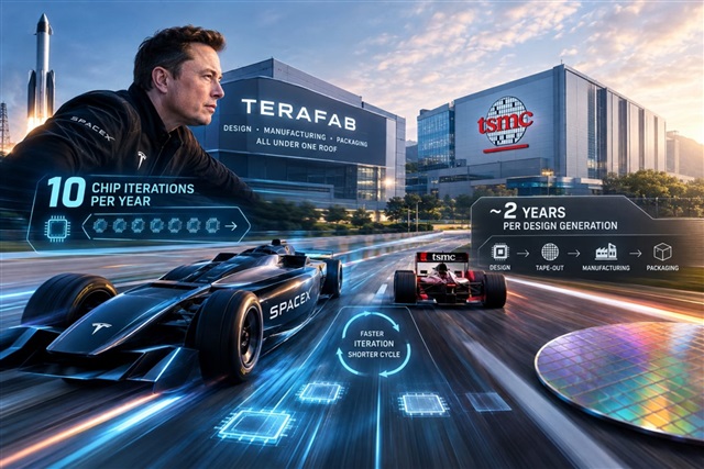
Speaking to more than 2,000 Tesla owners and investors at the X Takeover event held at Tesla's Gigafactory in Austin, Texas, on October 11, Elon Musk made a candid admission: "To be clear, I don't know how to make chips." He immediately followed it with a declaration: "We'll figure it out."
From automobiles to rockets, Musk has long favored setting ambitious goals first and then directing his teams to find ways to achieve them. Now, he intends to extend that approach to semiconductor manufacturing.
Musk has proposed developing chips using a methodology similar to rocket manufacturing, integrating multiple semiconductor processes within a single facility through his Terafab initiative and targeting 10 chip design iterations per year.
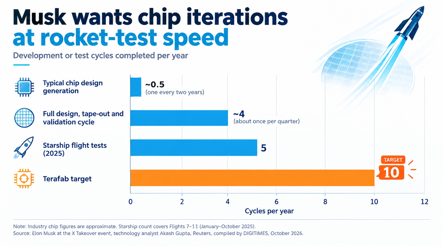
The target is aggressive compared with the industry's typical development cycle of approximately two years per design generation, raising questions about which limitations Musk hopes to overcome and whether his approach could challenge established semiconductor manufacturing practices.
Credit: Jerry Chen
Bringing SpaceX-style rapid iteration to chips
Developing a chip from initial design to mass production often takes several years.
Even after the design is completed, it must undergo tape-out, testing, and process adjustments. If the chip's actual performance falls short of expectations, engineers must revise the design, conduct another tape-out, and repeat the validation process.
It is precisely this repeated cycle of design and verification that Musk hopes to shorten dramatically.
The approach resembles SpaceX's Starship development program, which relies on continuous testing, data collection, and design modifications to identify problems quickly and apply the findings to subsequent development cycles.
Musk said Tesla and SpaceX will collaborate on semiconductor manufacturing, pursuing high-risk, high-reward technological experimentation.
The goal of producing 10 chip design iterations annually is primarily intended to accelerate manufacturing and testing cycles, rather than to bring 10 entirely different chip designs into mass production each year.
Musk explained that the team could rapidly test a chip, produce a new photomask, and manufacture the next iteration without interrupting the development process through prolonged waiting periods.
Although most approaches explored during the initial stages could fail, increasing the frequency of testing could help accelerate research and development.
Putting design, manufacturing, and packaging under one roof
Musk formally announced the Terafab project in March 2026, outlining an initial investment exceeding US$15 billion, with SpaceX, Tesla, and other companies participating.
Tesla and SpaceX have since named a site in Grimes County, Texas, on the former Gibbons Creek power plant site, where they said in August they would invest US$16.8 billion in a first phase. County filings in May cited an initial outlay of about US$55 billion and up to US$119 billion across all phases. Texas filings list construction starting around December 1, 2026, with the first phase to be completed by the end of 2028.
Intel joined the project in April 2026 as a manufacturing partner. The companies have so far agreed only to a general framework, and financial terms, intellectual property rights, and the continued participation of Intel and Tesla remain subject to later agreements.
The initiative seeks to integrate chip design, manufacturing, storage, and packaging within a single facility.
The facility is planned to produce chips for Tesla vehicles, Optimus humanoid robots, and Cybercab, as well as for SpaceX's planned space-based data centers. Samsung's fab in Taylor, Texas, is currently producing Tesla's AI5 chip, and Samsung has a US$16.5 billion deal to build the AI6 chip. TSMC supplies the rest of Tesla's chips.
Access to advanced lithography equipment is another constraint. ASML said it expects to ship more than 60 low-NA EUV tools in 2026, about 25% more than in 2025, with High-NA tools counted separately. A High-NA tool has reportedly cost EUR350–400 million, and orders are reportedly delivered 12 to 18 months after they are placed.
Musk also proposed using customized manufacturing equipment and faster design iterations to compress the overall timeline from chip development to production.
Yet his ambitions for development speed are even more aggressive than his plans for customized equipment. He wants to bring logic chips, storage, packaging, and photomask production together at one site, allowing chip design, manufacturing, testing, and revisions to be completed internally wherever possible. The ultimate objective is to achieve 10 design iterations annually.
If the development cycle could be shortened from one chip design generation every two years to 10 iterations per year, the approach could prove highly attractive to engineers by creating more opportunities to experiment with new technologies.
The real value of faster iteration, however, lies in reducing the waiting time between chip design, tape-out, and testing, enabling the results of each validation cycle to be incorporated rapidly into the next design.
Nevertheless, faster development does not necessarily translate into a competitive advantage. One of the biggest challenges facing Musk's vision of manufacturing chips at "light speed" is cost.
Photomask costs pose a major obstacle
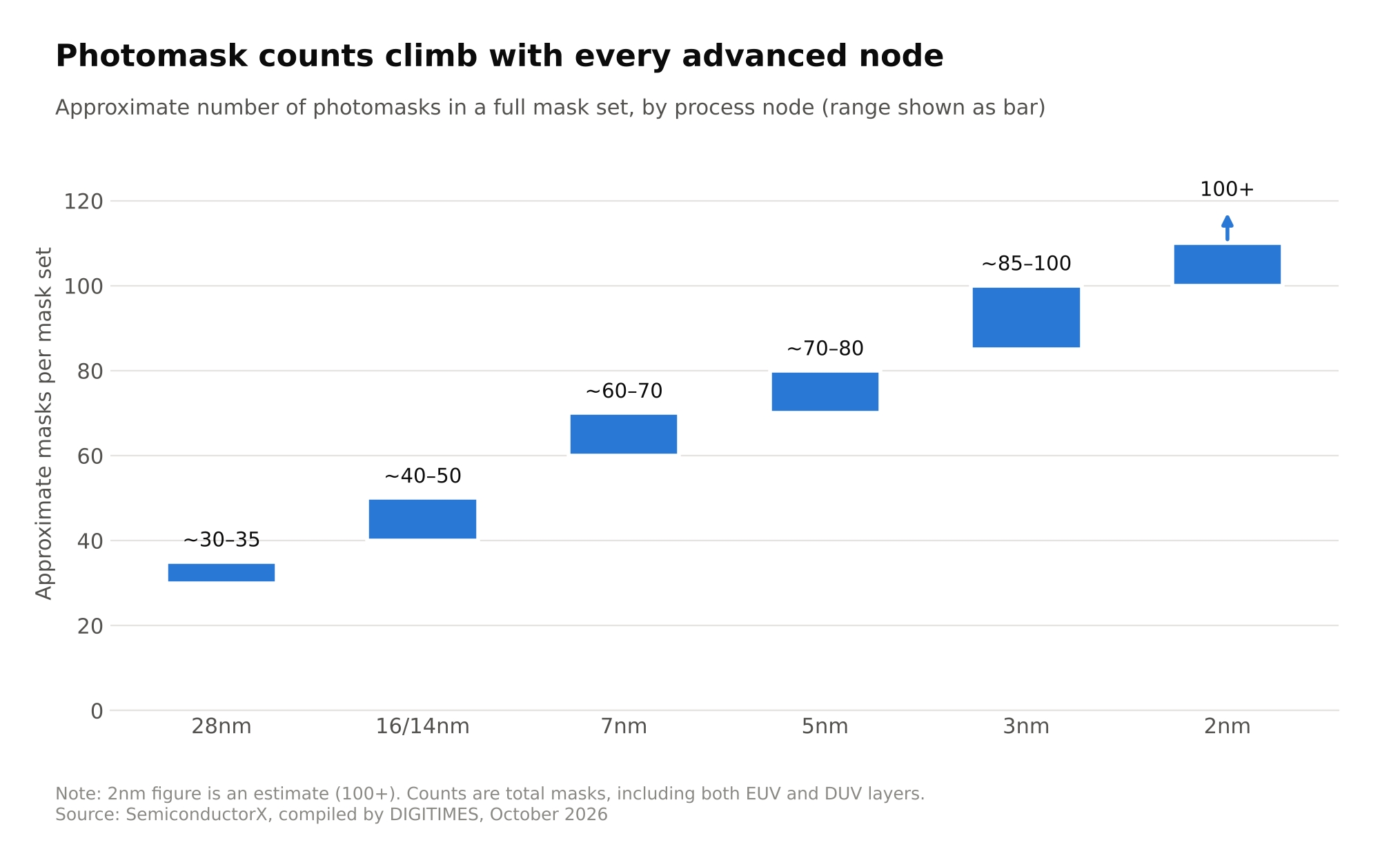
As semiconductor manufacturing processes continue to advance, photomask requirements and production complexity are increasing. For example, 3nm manufacturing uses approximately 24 photomask layers, compared with around 14 for 5nm processes.
Credit: Jerry Chen
Upfront photomask expenses for advanced nodes can run into tens of millions of dollars, with a single 3nm photomask set potentially costing between US$5 million and US$20 million.
If Terafab completes 10 chip design iterations annually, with each iteration requiring multiple revisions, photomask production and tape-out expenses could accumulate rapidly. That is before accounting for the additional time and capital required for process adjustments and yield improvements.
As Musk's concept moves toward practical implementation, managing the photomask costs associated with high-frequency design iteration will become a critical challenge.
Despite these obstacles, Musk continues to emphasize that Terafab will pursue high-risk, high-reward technological experimentation.
If the project succeeds in substantially shortening the time between chip design and manufacturing, it could challenge established semiconductor development models and potentially establish competitive advantages in testing speed and cost.
Can Terafab overcome lengthy validation cycles?
Technology analyst Akash Gupta noted that much of the time involved in a two-year chip development cycle is spent not on designing the chip itself, but on verification.
At advanced process nodes, photomask expenses can reach tens of millions of dollars. Meanwhile, wafers must pass through more than 1,000 manufacturing steps, and the fabrication process alone can take three to four months.
As a result, most chip design teams can complete a full design, tape-out, and validation cycle only about once per quarter, with each round of verification potentially costing millions of dollars.
If Musk's vision becomes reality, Terafab could significantly reduce the cost of repeated experimentation, creating a development model resembling SpaceX's approach to rocket engineering. Because SpaceX can manufacture rocket engines at relatively low cost, failed tests do not necessarily prevent the company from advancing development through rapid iteration.
Applying a similar model to semiconductors would require Terafab to make repeated chip design and manufacturing cycles substantially faster and less costly.
How Terafab would compete with TSMC and existing suppliers
TSMC raised its 2026 capital spending guidance to US$60–64 billion, up from US$52–56 billion, and expects spending over the next three years to rise by more than it did over the previous three.
Building fabs also takes time. TSMC's fabs in Taiwan take about two years to build, according to Tom's Hardware, while the first module of its Arizona fab took nearly five years, which the report attributes to labor issues, rising costs and cultural barriers.
Chip designers can already iterate without owning a fab. TSMC's CyberShuttle service lets several customers share one multi-project mask set, which reduces the tooling cost of prototypes. TSMC claims that prototyping costs can be cut by up to 90%.
During the X Takeover event, however, Musk did not provide a specific timeline for achieving this objective, saying only that it could take several years. Although Terafab still faces considerable challenges involving costs, technology, and execution, Musk's ambition to break through the semiconductor industry's established development cycles is clear.
Article translated by Scarlett Yu and edited by Jerry Chen