


At the China International Optoelectronics Expo (CIOE), a palm-sized metal transceiver represents the shift from copper to light in data center infrastructure, one of the biggest transformations in the industry amid the AI boom.
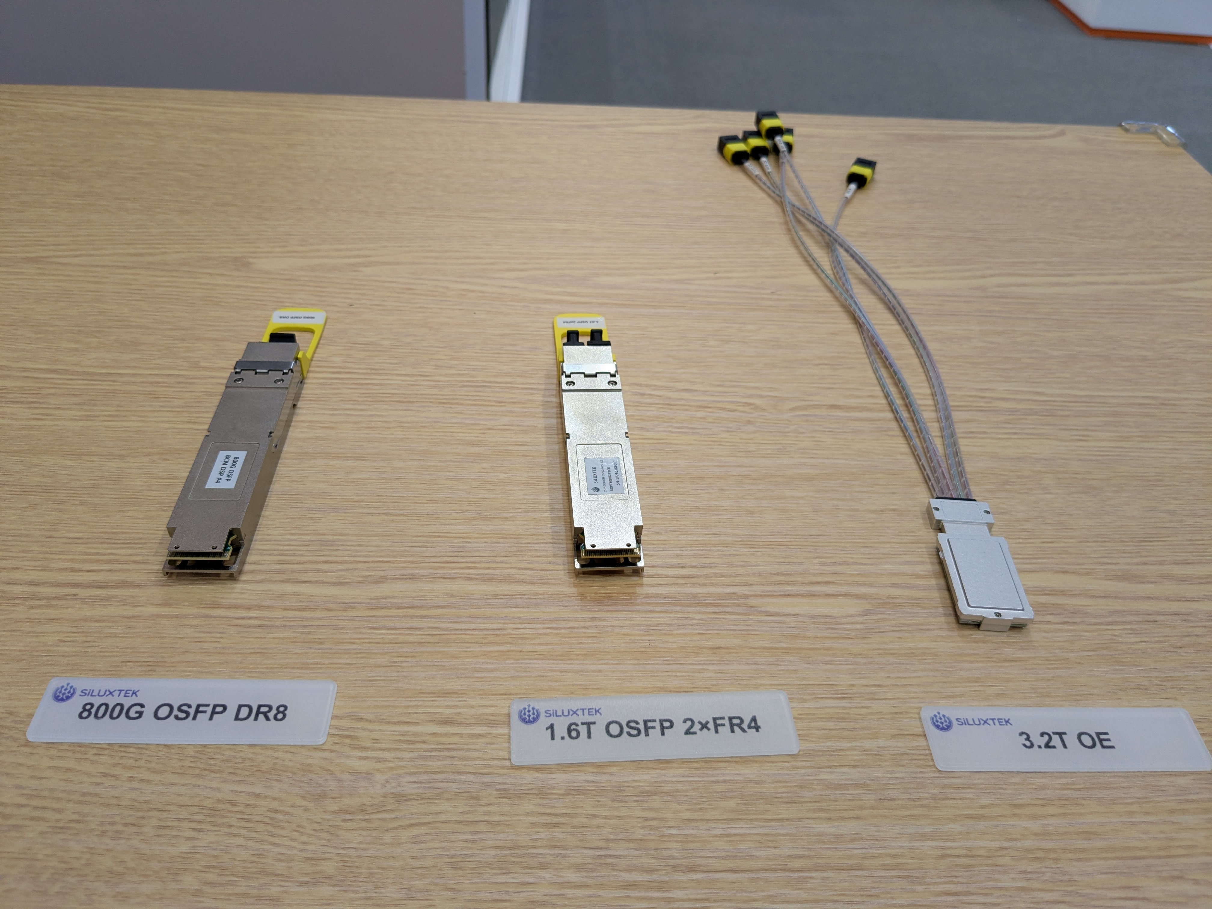
The device, an 800G optical transceiver built on GlobalFoundries' silicon photonics technology, is a fully retimed dense block of metal and cooling fins wrapped around a digital signal processor (DSP) drawing roughly 20 watts.
According to Thomas Barber, Vice President of GlobalFoundries' Data Center and Communications Infrastructure business, the device illustrates the thermal challenges reshaping the industry: "As we increase the data rate, power consumption goes up, and it doesn't necessarily go up linearly."
"It's harder to drive data faster, so you have to put more energy into digital processing and lasers," he said. "So that just makes the power consumption problem get worse."
GlobalFoundries' presence at CIOE centers on two product lines: silicon photonics chips that process light, and silicon germanium chips that handle the transimpedance amplifiers (TIA) and drivers converting between electrical and optical signals.
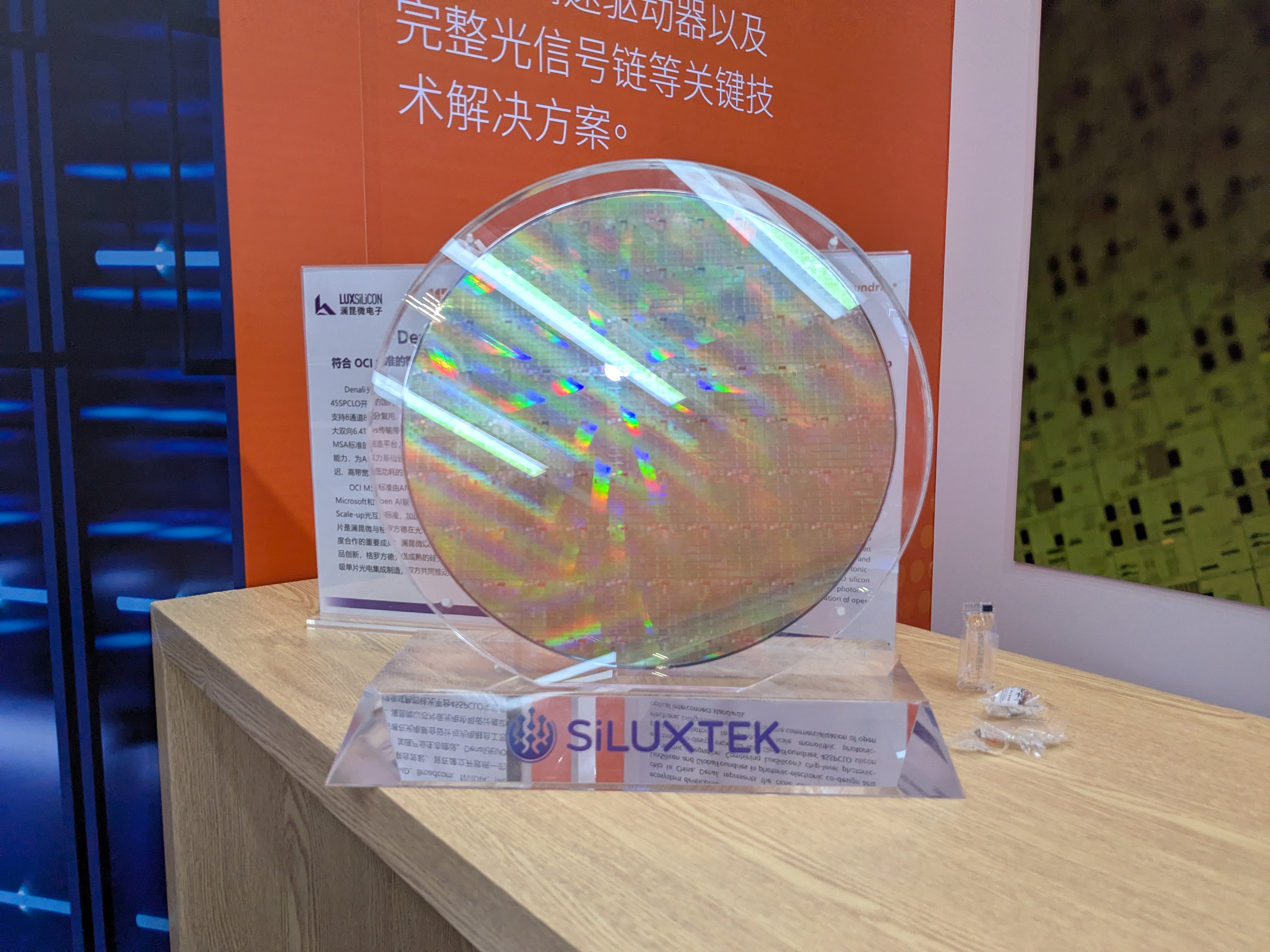
One is its monolithic photonics process, which includes an optical I/O chip from Luxsilicon that combines CMOS electronics and photonics on a single die to perform the full electronic-to-optical conversion in one chip. The other is a family of pluggable transceivers built with Siluxtek, a partner that fabricates photonic ICs on GlobalFoundries' technology using 300mm wafers.
Most of the industry still runs on 200mm wafers, Barber noted, a legacy of an era when demand for silicon photonics technology was modest. GlobalFoundries' move to 300mm wafers, which results in more than double the gross die per wafer, is driven by the recent surge in optical transceiver demand tied to 800G and 1.6T networking.
Credit: DIGITIMES
The copper-to-optical tipping point
Barber explained that demand for silicon photonics is about to steepen dramatically. A current bottleneck in AI infrastructure lies in the scale-up network — the dense web of copper connections tightly coupling GPUs within a rack — which is currently capped at around 72 GPUs per rack.
Two developments are driving the transition from copper to optics. One is that scale-up networks are expanding beyond the single rack to grow past these 72 chips. Another is a growing need to increase the data rate beyond 400G per lane. These are leading to rising demand for optical interconnects both between and within racks.
Barber added that this physical limit is forcing a wholesale shift from copper to optical interconnects for scale-up networking, which contains roughly ten times the bandwidth demand of scale-out networks.
"The bandwidth of the scale-up network is roughly 10 times higher than the scale-out network that uses optics today, so this transition drives a 10-times increase in the demand for optics," he said. "Not a lot of markets grow 10 times, and it can happen within the next five years."
At the event, GlobalFoundries said it was also keeping an eye on new manufacturing trends emerging across the industry in China. Barber pointed to the rapid rise of near-packaged optics (NPO), a design that shrinks four to eight pluggable transceivers into the same size and moves optical components from the edge of a server into its interior. Barber said this shift could take hold industry-wide within the next year.
Today's commercial products run at 200G per second per optical channel, but Barber expects 400G per channel to be a major focus in the field by this time next year. This will require advances on both the photonic and electronic sides of the technology.
Credit: DIGITIMES
A research boost for pushing lane limits
When asked about the US Department of Commerce awarding the company US$300 million in July to accelerate silicon photonics research, he continued that the funding will go toward pushing past current 200G-per-lane limits using alternative materials such as thin-film lithium niobate (TFLN) and barium titanate (BTO).
It will also be used to develop 2.5D and 3D chip-stacking techniques for co-packaged optics (CPO) within the US under the company's SCALE platform that was announced in May. This will allow for heterogeneous integration to build full-scale optical engines.
When it comes to integrating lasers with silicon, Barber said that the industry has not seen a large drive for that kind of integration so far. Because silicon is a poor material for generating light, manufacturers still rely on separate indium phosphide lasers placed alongside photonic chips rather than fully integrating them. This is partly for ease of replacement and reliability testing, and partly because lasers are sensitive to the intense heat generated by GPUs in co-packaged designs.
Despite talk of an AI infrastructure bubble among the public, Barber remains confident that the rapid growth currently seen in the market will continue for at least a few more years: "It's a bubble when capacity starts to outstrip demand, and no matter how much we invest in data centers, they are full the minute they're built."
With the market for silicon photonics growing 1.5 to 2 times annually, he said that GlobalFoundries intends to expand manufacturing capacity at or above that pace, including deeper collaboration with Taiwan's manufacturing and packaging ecosystem and continued partnerships with Chinese firms such as Zensemi as given nodes grow in popularity.
Article edited by Jerry Chen