
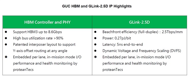
Global Unichip Corp. (GUC), the Advanced ASIC Leader, announced today that it has successfully taped out a test chip with an 8.6Gbps HBM3 Controller and PHY and GLink 2.3LL for AI/HPC/xPU/Networking applications. GLink 2.3LL die-to-die interface provides best-in-class power, performance, and area (PPA) with 5ns end-to-end latency, 5Tbps/mm beach-front (2.5T full-duplex) and 0.27pJ/bit power efficiency. The test chip is taped out at the TSMC 3nm process and adopts the TSMC CoWoS advanced packaging technology.
GUC's HBM3 Controller and PHY IPs are available at TSMC's 7nm and 5nm process nodes supporting both CoWoS-S and CoWoS-R technologies. The IPs were validated with both SK hynix and Samsung HBM3 memories GUC's HBM3 Controller demonstrated higher than 90% bandwidth utilization at random access.
GLink 2.3LL supports TSMC's InFO_oS and CoWoS-S/R technologies. It had already been silicon-validated at TSMC's 5nm process node. GUC provides full AXI, CXS, and CHI bus bridges with configurable parameters using the GLink 2.3LL physical interface. The GLink 2.3LL I/Os' high cross-talk tolerance allows CoWoS/InFO unshielded routing, effectively doubling the number of signal traces of the interposer or RDL.
Both HBM and GLink have integrated proteanTecs' interconnect monitoring solution to provide high visibility for testing and characterizing the PHY, and to enhance the end-product with in-field performance and reliability observability. With this tape out at 3nm, the GLink/HBM IP portfolio is now available in TSMC's 7nm, 5nm and 3nm technologies, which have been adopted by AI/HPC/Networking clients in their products.
"We are proud to be the world's first company to tape out an 8.6Gbps HBM3 controller and PHY IP as well as the most efficient die-to-die interface GLink 2.3LL at 3nm technology," said Dr. Sean Tai, president of GUC. "We have now established a complete 2.5D/3D chiplet IP portfolio for advanced technology up to 3nm. Together with design expertise, package design, electrical and thermal simulations, DFT and production testing on TSMC 3DFabric, a comprehensive family of 3D silicon stacking and advanced packaging technologies including TSMC-SoIC, CoWoS, and InFO, we provide cutting edge solutions to our customers and assist them to achieve even greater success in their products and businesses."
"We keep delivering best-in-class die-to-die interfaces enabling a chiplet revolution. Our IPs span through all TSMC's advanced process and 3DFabric technologies. Convergence of 2.5D and 3D packaging using HBM3, GLink-2.5D/UCIe and GLink-3D interfaces enables highly modular, chiplet-based, much bigger than reticle size processors of the future," said Igor Elkanovich, CTO of GUC.
To learn more about GUC's HBM3/2E, GLink-2.5D/3D IP portfolio, and InFO/CoWoS/3DIC total solution, please contact your GUC sales representative directly or email guc_sales@guc-asic.com
Source: Company

