
KLA is proud to be part of the most significant technological breakthroughs that help create the devices and ideas that transform our current life and shape our future. One of the latest emerging trends is a renewed focus on microLED technology.
What is a microLED, and why is the industry focusing on this technology?
As the name suggests, a microLED, or µLED, is a light-emitting diode (LED) – roughly 100 times smaller than conventional LEDs. MicroLEDs can be arranged into arrays to make high-resolution displays for applications ranging from smartwatches to very large displays – unlike conventional LEDs, which are suitable only for very large displays like billboards or stadium screens.
MicroLED technology was invented in 2000. However, it wasn't until 2012 that a major consumer electronics company demonstrated a 55-inch, high-definition microLED TV. Other companies followed with their own demonstrations in 2018 and 2019 at retail prices of $80,000 for 89-inch models, making the technology out of reach for most consumers. Although microLED can potentially offer significant advantages over LCD or organic light-emitting diode (OLED) screens, technology issues and production costs have prevented widespread commercialization.
KLA – which has supported the global display industry for more than 40 years – has during the past decade been helping leaders in microLED technologies to overcome many of the obstacles to mass production and reduced costs.
"Our proven process and process control products are designed to meet the unique and demanding challenges of the complex microLED production flow to help accelerate wide market adoption," said Chet Lenox, KLA fellow, industry and customer collaboration.
While more products, based on slightly larger "miniLEDs" (typically ~50µm-300µm square), have been brought to market successfully in recent years as a way to improve on traditional LED backlighting for LCD displays, screen manufacturers and their supply chain are still committed to developing the more advanced microLED technology. In addition to the key goal of reducing product cost for consumers, companies are investing heavily in microLEDs for use in small products like watches and augmented reality (AR) headsets because they deliver better energy efficiency, consistent pixel quality and other key benefits as shown in the graphics below.
The potential market is huge. Shipping for microLED displays is expected to total 5 million and generate $7 billion in revenue by 2025, rising to more than 11 million units shipped in 2027, according to global technology research firm Omdia.
A key factor behind the industry's focus on microLEDs is that LCD and OLED displays are produced on large substrates, where all layers are deposited one after the other. The larger the substrate, the more efficient the process – but large single displays can be difficult to handle and ship. MicroLEDs displays, however, can be produced using seamless tiling of small modules into larger displays.
Comparison of MicroLEDs, OLED and LCD Displays
The schematic cross-section of a typical microLED display (below) shows the simpler and thinner structure of a microLED compared to a thin film transistor liquid crystal display (TFT LCD) or OLED display, with the red/green/blue LED chips and a single electrode encased between the substrate and glass cover. The precise arrangement of the red, green and blue sub-pixels will vary among models and may even be stacked on top of each other.
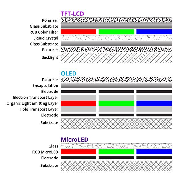
Schematic (not to scale) cross-section through a typical TFT LCD, OLED and microLED pixel illustrating the relative simplicity of a microLED display.
MicroLEDs offer viewing performance equivalent to or, for some criteria such as brightness and refresh rate, better than OLED and LCD technologies. They also offer a longer life than OLED, thinner packaging and generally better energy efficiencies.
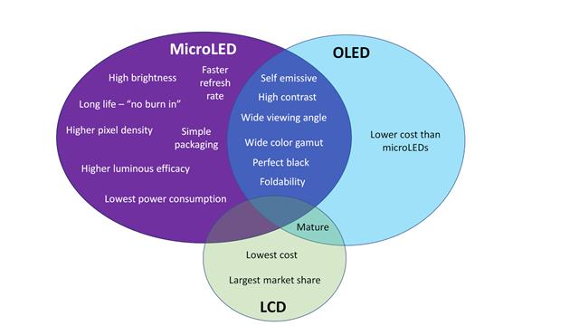
Relative benefits of microLEDs versus TFT LCD versus OLED technologies and where they overlap.
The industry must overcome significant manufacturing challenges to achieve acceptable yields and a viable cost point, including:
*Baseline yield optimization at each process step
*Selecting known good die with fully functioning red/green/blue microLEDs to be transferred
*Flawless backplane circuit design and patterning – in-process inspection, testing and potential repair
*Mass transferring millions of micro-sized red, green and blue microLEDs in the desired arrangement and precise locations (Solutions to avoid this might include the use of white or blue microLEDs with color conversion, growing uLEDs directly on silicon backplanes or using wafer-bonding of epi layers on the backplane.)
*New manufacturing technology adoption, new supply chains and cost of change
KLA Solutions for MicroLED Manufacturing
Each of the above would seem to add cost and make LCDs and OLEDs more economical. However, KLA's metrology, inspection, wafer processing and repair solutions are critical to helping microLED manufacturers address these challenges, optimize yields, reduce the need for built-in redundancy and reduce expenditures to help microLED displays become a viable alternative to the established technologies.
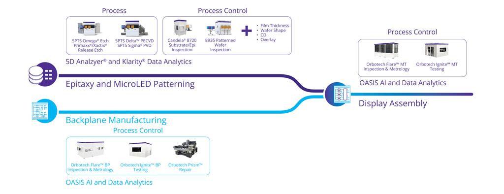
KLA's comprehensive portfolio of solutions for microLED manufacturing provides a pathway to yield improvement throughout the entire process – from epitaxy wafer to final display. KLA's proven process and process control products are designed to meet the unique and demanding challenges of complex microLED production.
Author: Carolyn Short, technical communications manager, EPC Group, KLA